The iconic Neumann KM84 is a legendary vintage SDC microphone that many people seem to prefer over the modern KM184, as it allegedly sounds more natural and balanced than its successor model. I’ve listened to several KM84 vs KM184 shootouts on Youtube and I cannot say which one I would prefer. It all depends on what is being played. The KM184 gives a tad more sense of detail in the upper octaves. But in this shootout (oops, the link is dead…), I found the off-axis response of the KM184 somewhat hollow and disappointing. Anyway, because of this reputation, building a KM84 clone has become a popular DIY project, and several kit suppliers offer complete kits that are supposed to give a similar sound as the original KM84. Note: I do not have any experience with such kits, nor will I commend any of them because I don’t have any hands-on experience with them. Just read all the reviews and relevant threads on, e.g. GroupDIY.com. Or just listen to this shootout on YouTube, where a Neumann KM84 is compared with a DIY clone with 3U capsule and Cinemag transformer. To me, they sound identical, but I’m the first to admit that I don’t have Golden Ears.
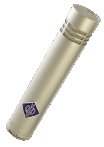
The legendary Neumann KM84
Next to the legendary sound quality of the KM84, another reason why the circuit is cloned so often is the fact that it is straightforward to build. With just a single JFET and a transformer, it is easy to build for beginners. And it will fit into a popular MXL 603S or similarly sized pencil mic when built with through-hole components. This could indeed be a valid reason to choose the simple KM84 circuit, but many people also relate its simplicity to quality, which I believe is factually wrong. Simplicity comes with performance limitations, which will become obvious when reading this article. And tell me, if this would really be such a good design, why did all the name brands move on and design much more complex circuits for their newer microphones? And would you really prefer a simple T-Ford over a contemporary car and call the T-Ford better…? As said, this circuit comes with some limitations, which one should be aware of when building or modifying a KM84 circuit. Or you just avoid these limitations altogether and choose another, more complicated circuit that has them resolved. I have walked both paths and first built a KM84 style circuit that stayed close to the original design and which served as a reference to other builds, then made a handful of other (proprietary) charge-amplifier designs to find out whether there are measurable and audible differences and to find out which one I would prefer. The KM84 style circuits I have named the KM84+ and KM84++ are further described here.
Let’s first explore how the KM84 circuit works. I could try to explain that, but it has already been done before, so I will just provide the link to two URLs where they are explained. So if you have no clue yet what a charge amplifier is and you want to learn more about the KM84 circuit basics, I would encourage you to open and read the URLs below.
https://en.wikipedia.org/wiki/Charge_amplifier
(Notes: This article explains the Charge Amplifier concept using an Op-Amp. If you want to understand the synergies with the KM84 circuit, think of the JFET as an Op-Amp, with Gate = inverting input, Source = non-inverting input, and Drain = output. Replace the sensor in the schematic with the microphone capsule.)
https://audioimprov.com/AudioImprov/Mics/Entries/2015/4/23_Basic_FET_Microphone_Circuits.html
(There are some details in the circuit description that I do not agree with, but for a basic understanding of the circuit, it is fine.)
Now that you understand the KM84 circuit basics, we can examine the effects of changing various component types and values and explore how they affect Gain, THD, Frequency Response, and noise, i.e. how they affect the sound of your KM84 build. For the quick readers who are not interested in knowing all the background details, scroll all the way down to the Conclusions section. Let’s start by examining the effects of capsule capacitance and the coupling capacitor C1. Btw, I expect many things being covered in this article to also apply to other single JFET stage impedance converter designs, such as the classic U87 and all of its derivatives.
Capsule capacitance and C1
To determine the effect of the component values on the circuit properties, I used the LTspice circuit below. I have parameterized the component values whose effects I wanted to investigate. Though most likely the capsule and its capacitance will be a given when you start building your clone, it’s interesting to see how it affects the gain and noise.
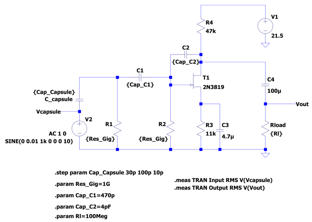
To determine the A-weighted output noise, I added an A-weighting filter to Vout, which is not shown in the schematic. Btw, the A-weighting filter is just the circuit published by Elliot Sound Products using LTspice’s noiseless resistors and voltage-controlled voltage sources as ideal op-amps.
Keeping all other component values as depicted above, sweeping the capsule capacitance from 30 pF to 60 pF resulted in the Gain and Noise voltages listed in the table below. As can be concluded from the table, the output RMS Noise voltage is not much affected. But due to the increasing gain, larger capsule capacitances are beneficial for the total system SNR determined by the input referred noise. E.g., if you swapped a 39pF Takstar CM-60 capsule for a 53.5 pF 3U Audio Cardioid capsule, you would gain ~2dB SNR improvement from the circuit. However, with SDCs, capsule self-noise is often dominant, so whether this improvement turns out to be audible remains to be seen.
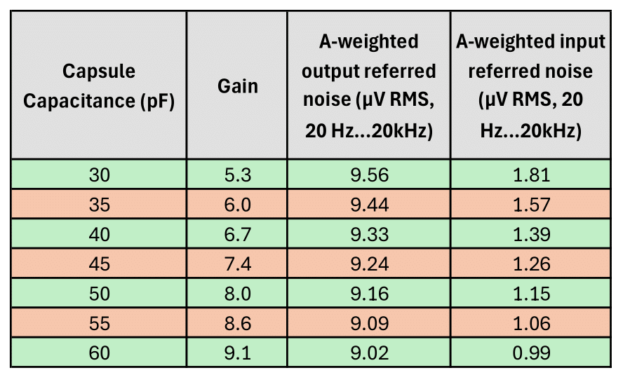
Gain and Noise as a function of Capsule Capacitance
Before we move on to C1, let’s first check whether the simulations yield any meaningful results before accepting them blindfolded as true. For this, we need to know the KM84’s capsule capacitance (36 pF), sensitivity (= 10 mV @ 94 dBA SPL), and self-noise level (17 dBA SPL). From the sensitivity and self-noise level, we can calculate the equivalent output noise of the microphone, which includes both the capsule self-noise and the noise from the electronics. The noise from the electronics should be equal to or lower than the microphone output noise, of course. Let’s calculate both and compare:
Noise from electronics: The nearest capsule capacitance from the table equals 35 pF, where we find 9.44 μV output noise. This is specified at the output of the JFET stage, so on the secondary of the 7:1 transformer, it is equal to 9.44 / 7 = 1.35 μV. (The transformer is assumed to be noiseless.)
KM84 self-noise: The output noise level is 94 -17 = 77 dB lower than the 10 mV reference level, which equals 10 mV / (10^(77/20)) = 1.41 μV.
We find that the noise from the electronics is indeed slightly lower than the total noise from the microphone, so we can safely assume the simulations are close enough to the truth. Nice! 🙂
Now let’s see what C1 does to the Gain and Noise. As C1 acts as a coupling capacitor, it will be obvious that you’ll want the capacitance to be much higher than the capsule capacitance to avoid a capacitive voltage divider effect. But how much can be gained if we choose a capacitor value greater than the typical 10 times the capsule capacitance? Let’s assume a capsule capacitance of 40 pF, which is close to the Takstar CM-60 capsule capacitance. And let’s keep the remainder of the circuit as depicted above. The results:
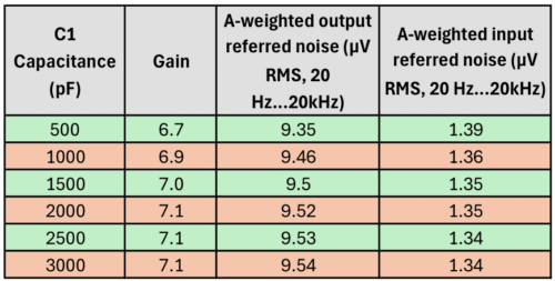
Gain and Noise as a function of C1
The Gain increase and Noise improvements are not spectacular, as could be expected, but could still be worthwhile if done in combination with other improvements. Assuming C1 is an NP0/C0G capacitor, changing from the standard KM84 value of 470 pF to e.g. 2200 pF will only cost you a few cents at most and will get you ~0.5 dB more gain and ~0.3 dBA better SNR. If using a higher capacitance capsule, e.g. the one from 3U, then you’ll want C1 to be much larger than 470 pF. I typically used 1000 pF when designing SDC circuits, but that will change to 2200 pF from now on. However, you should be aware that there is a drawback to increasing the capacitance, especially in combination with increasing R1 and R2, as discussed in the next paragraph. It will take much longer to charge this capacitor at power up, and during the charging process, the JFET will not pass audio. E.g. with 2200pF and 5G resistors, it can take up to a minute before the microphone passes audio. So you’ll have to consciously choose the right balance between low noise and a short power-up time.
R1 and R2, Frequency Response & Noise
As most will have understood, R1 is the resistor through which the capsule capacitance is charged from the polarization voltage supply. This supply is not shown in the LTspice schematic, but R1 is connected to the ground for AC signals in the audio band through a decoupling capacitor of 10…100nF. R1 typically ranges from a few hundred MΩ, up to 5 GΩ. In most cases, R1 = R2 = 1GΩ. R2 provides a leakage path for the Gate bias current to the ground or a bias voltage.
Assuming C1 >> C_Capsule, we can consider R1 and R2 to be in parallel for audio signals. The capsule capacitance, together with R1//R2, forms a high-pass filter. Assuming a 40 pF capsule and R1 = R2 = 1GΩ, the cut-off frequency equals 8 Hz. That’s well below the audible range; in most cases, a lower cut-off frequency would not be required. But…. there is another reason you might want an even larger resistance value, resulting in an even lower cut-off frequency. The reason is noise. Resistors generate thermal noise (aka Johnson noise), and though it sounds counterintuitive, increasing the resistor value will actually reduce the noise from the circuit. The reason for this is that the Johnson noise of the resistor increases with the square root of the resistance, but at the same time, the amount of noise that is shorted to ground via the capsule capacitance increases proportionally with the resistance. Or, saying it differently: with each doubling of the resistor values, the low-pass frequency above which noise is attenuated will halve. The graphs below clearly demonstrate both effects.
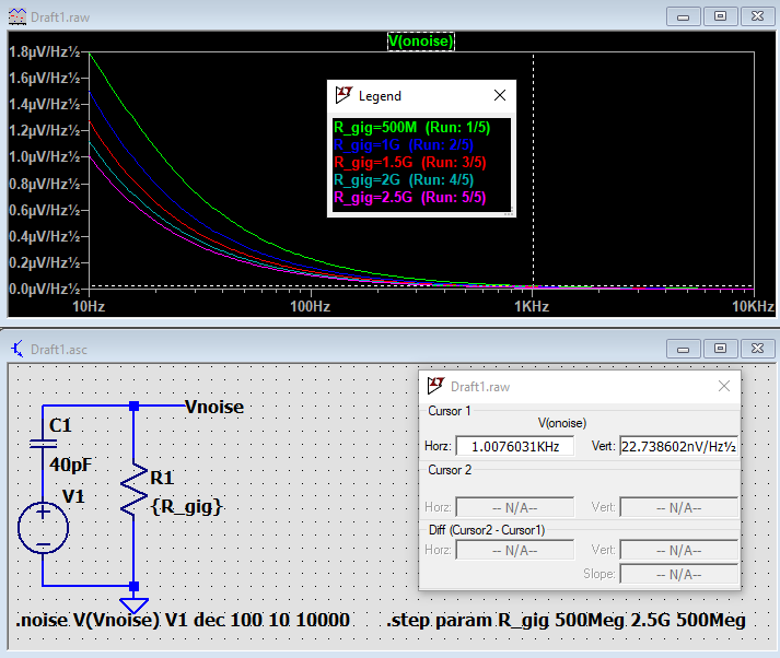
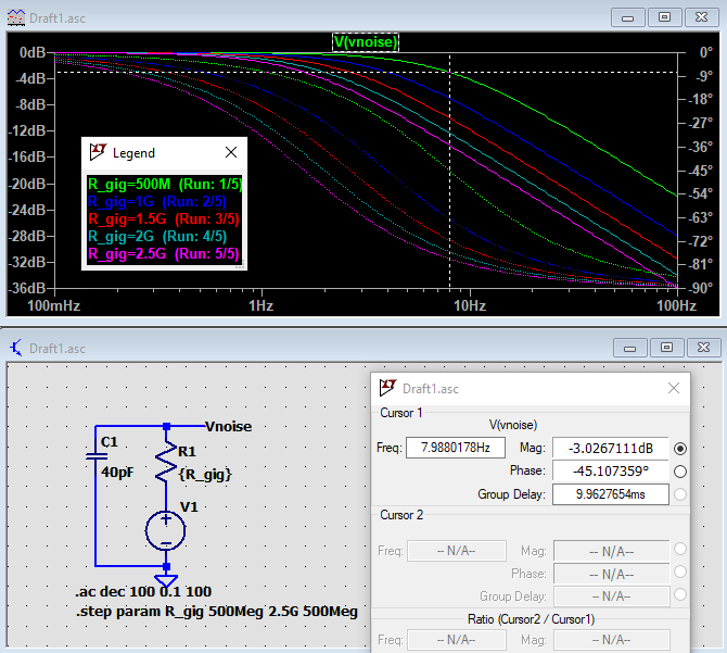
Next, we’ll see what this resistor noise does to the total circuit noise. Therefore, we go back to the LTspice circuit from the beginning of this chapter and sweep the values of R1 and R2 from 1G to 5G in 1G steps. Note: I’ve now added a transformer to the circuit, resulting in slightly different noise figures compared to the simulations above.

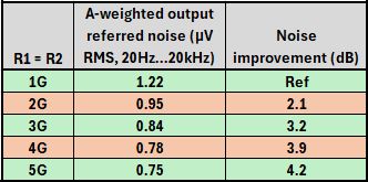
A-weighted output-referred noise as a function of R1 and R2.
From the graphs and the table, it is obvious that a major improvement can be made when R1 and R2 are stepped up to 2G or even 3G. In practical JFET impedance converter designs, most low-frequency noise, say below several kHz, originates from these resistors. Luckily, due to the low sensitivity of the human ear to low frequencies, high LF noise figures are not as objectionable as one would first think. Unfortunately, this noise improvement of the electronics will not translate into the same noise reduction of the microphone as a whole due to the self-noise of the microphone capsule. Adding the capsule noise into the equation, the A-weighted noise figure of microphones can be reduced by 2 or more dB when increasing R1 and R2 to 3G or even 5G from the standard 1G.
JFET selection and JFET bias
The JFET impedance transformer basically consists of a Common Source amplifier, whose closed-loop gain is determined by the capsule capacitance and C2. If the open-loop gain were infinite, then the gain would have been equal to C_capsule/C2. But as we’ll see further down in this section, the actual open-loop gain is just a few times higher than the required closed-loop circuit gain, and consequently, the closed-loop gain cannot be accurately calculated by the simplified formula above. And with the open-loop gain of the JFET CS amplifier being proportional to the widely varying JFET common source transconductance gm (or gfs), it also means that the closed-loop gain can vary from microphone to microphone, making it difficult to find matched pairs of microphones. Add to this the normal component tolerances of the capsule capacitance and C2 and the closed-loop gain can easily be off by more than 1 dB between two microphones. This is one of the reasons I designed a KM84 variant with an adjustable polarisation voltage generator, which allows you to trim the circuit gain, including the capsule, and make gain-matched mic pairs without hand-picking components.
From the above, and the KM84 circuit topology, we can define some requirements for the JFET to use. These include:
- High transconductance (gm) for high open-loop gain and accurate closed-loop gain.
- Max Vds at least 25V. At a higher Vds working voltage, JFETs become noisier. This is less prominent with a device with a high maximum Vds.
- Low Gate-Drain capacitance, so it’s easier to define the closed-loop gain accurately through C2.
- Low output conductance (gos), i.e. high Drain-to-Source impedance. (This limits the open-loop gain, as we’ll see later.)
- Low noise, of course.
Unfortunately, these requirements are contradictory, so you won’t find many suitable devices on the market. But one such device that meets these requirements is the 2N3819, also used by Neumann in the KM84. This is a through-hole device and is still made by Central Semiconductor, but some say they are not as good as the original ones from, e.g., Vishay or Fairchild/onsemi. But what exactly they dislike about the Central Semi part, they do not tell. When looking for a suitable SMT device, I ended up using the onsemi MMBFJ309LT1G. Next to the MMBFJ309LT1GI tested the 2SK209, 2SK209, CPH3910 and 2SK2394. More JFETs were tested by member Voyager10 on GroupDIY and published in post #74 and beyond in this thread. The ORS87 circuit used in these tests is also a KM84-style charge amplifier, but with a modified feedback circuit and different working voltage, which results in a different bias current for the lowest THD.
Assuming the Drain voltage is set to 10V, as stated in the Neumann KM84 schematic, the calculated bias current is only 240 µA, . This is one of the reasons the KM84 is a bit noisy: noise from a JFET is the lowest when Id is close to Idss, but should typically be at least 0.5…1 mA for most small signal JFETs. However, a very low bias current was required for this circuit to keep the phantom power voltage as measured on the XLR pins as high as possible. This had to be done because the capsule polarisation voltage is derived from the phantom supply voltage and has to be as high as possible for low noise and high sensitivity. The only way to get a high polarization voltage, AND at the same time bias the JFET amplifier at a high current for low noise is by adding a polarization voltage oscillator. This is exactly what I’ve done in a circuit which I called the KM84++ here. Running the JFET at higher bias currents would also allow the use of smaller transformer ratios, which would reduce odd-order harmonics. I can imagine there was no space inside the KM84 for such a polarization voltage oscillator, but I’m a bit puzzled why Neumann did not use that in all of their LDC designs where there’s plenty of space. Were they afraid of EMC issues? Did they want to keep the costs down? Did they think biassing the JFET at low currents and having high transformer ratios improved the subjective sonic qualities?
Anyway, whatever made Neumann decide to derive the polarization voltage directly from the phantom supply, thereby limiting the available current to bias the JFET, we also have to decide on what voltage to have on the Drain node. There has been a lot of discussion about this on DIY forums. The problem starts with the definition of what is better: do you want minimal distortion? Or do you want the circuit to clip symmetrically? Or anything in between? Should you adjust the bias just by listening or should you trust measurements? And if you decide to adjust for minimum distortion, then at which input level should this be done? Most people seem to adjust for minimal distortion, which will be found in the ~10-11V area. I think Neumann did that too. On the other hand, if minimum distortion is your goal, then why would you want a transformer-coupled microphone in the first place? I don’t have a strong opinion on this, but it’s something to think about when choosing between transformer-based and transformer-less microphones.
OK, sow we (or Neumann) decided on the JFET, the bias current, and Drain voltage, all of which are a result of the chosen concept of a Charge Amplifier and polarization voltage derived from the Phantom voltage. The question now is: can we dimension the circuit in such a way that we can directly drive a mic preamp with it? For that to be feasible, you’ll want an output impedance that is at least 5 times as low as the mic preamp input impedance, which would already give a 2 dB signal loss. So preferably, you want to aim for a factor 10 or more. With mic preamp input impedances typically in the 1-2.5 kΩ range, the output impedance should be no more than 200 Ω and preferably even lower. Referring to the LTspice circuit at the beginning of this page and taking a 40 pF feedback capacitor C2, to obtain an arbitrary unloaded 0 dB circuit gain, the simulated output impedance of almost 1800 Ω. Way too high to drive a mic preamp input directly! So we’ll need a second impedance transformer stage to bring the mic output impedance down to a usable value. Which brings us to the next paragraph…
The output transformer
As we’ve seen in the previous section, the output impedance of the JFET Charge Amplifier circuit is still too high to drive a typical mic preamp with an input impedance in the order of 1 kΩ – 2.5 kΩ. The signal loss would be too much. So we must add a second impedance transformer stage to obtain an output impedance of 200 Ω or less. In the 1960s, when Neumann developed the KM84, output transformers were the norm. Neumann chose a 7:1 transformer, which they called the Bv-107. With this transformer ratio, the mic preamp input impedance presents as a 7-squared increased impedance to the JFET output. So let’s say your mic preamp has an input impedance of 2 kΩ, then the JFET will see a ~100 kΩ load. The output impedance of the JFET stage is ~7k82, so this 100 kΩ is an acceptable load. However, this 100 kΩ is parallel to the transformer’s inductance, which does significantly load the JFET at low frequencies and should not be neglected. The inductance of ~50H presents a load impedance of ~6300 Ω to the JFET output at 20 Hz, roughly halving the output level at that frequency. More on this in the paragraph covering C4.
As far as transformers are concerned, we are quite limited to what is available at a reasonable price on the market. The original Neumann Bv-107 transformer is almost unobtainable. And if you find one, it’s unaffordable. So we have to look for an alternative with a turns ratio close to or equal to that of the Bv-107, that fits into our SDC tube of choice. Assuming a Ø 22mm body (e.g. MXL 603S, Takstar CM_60 or CM-63, Alctron T-02A etc.), at least the following types should work (in no specific order):
- 3U Audio GZT-84. Turns ratio 6.5:1. Other specs unknown. Available from the 3U Audio E-Bay shop. Seems reasonably priced.
- Moby BV107. Moby provided no electrical specs. Price unknown, not published on their website. Makes me fear for the worst…
- Cinemag CM-5722. They provide a rather detailed datasheet, which I like, but it’s lacking the primary inductance value. The turns ratio is 6.9:1. I don’t see this transformer listed somewhere in online shops and assume it must be sourced directly from Cinemag. Offered on Reverb for $100. Too much for me…
- TAB Funkenwerk / AMI T8 transformer. The datasheet is not as detailed as the Cinemag transformer, but they do at least specify the primary inductance value. Turns ratio 7:1. With a price of $120, I find it quite expensive.
- ASTDS T-8 from Aliexpress. Turns ratio 7:1, and no other electrical specs are provided. I measured a primary inductance of 58H, though that depends on how it’s measured. Primary resistance measured 220 Ω and secondary 22 Ω. With a price of just ~$20, it is very affordable.
Transformers, at least the good ones, can be expensive, but I did not want to invest heavily in them for my first KM84 circuit builds. So I decided to buy some ASTDS T-8 transformers from Aliexpress. And when they would sound good enough, I would just keep them in. Whether this is actually a good transformer or not and how it compares sonically to the others, I don’t know. Transformers and their sonic qualities are often the subject of discussion on audio forums, but to what extent they really do matter, I cannot tell. Maybe the differences are best noticed (or only noticed?) at extremely low frequencies and high SPLs, where one transformer might saturate and distort sooner than others. Anyway, blind tests of KM84 clones and an original Neumann KM184 revealed that many people had difficulties telling them apart despite their alleged sonic differences and measurably different frequency responses and THD figures. So I’ve become a bit skeptical about the importance of the brand and type of transformer used. I think it’s more important to match the circuit to what I think are the most important transformer properties: primary inductance and turns ratio (aka transformer ratio). The primary inductance determines the low-end frequency response, in conjunction with the output impedance of the JFET amplifier and the coupling capacitor C4. More about this in the next paragraphs.
C2, C4 and how they affect Gain, THD, and Frequency Response
With C2 and C4, we now arrive at the components that, next to the transformer, really matter to the sound. So these are typically components that you want to experiment with when you want to alter the microphone’s sound to your taste.
C2 and how it affects the Gain and Frequency Response
Capacitor C2 in the KM84 circuit constitutes the feedback capacitor Cf in the Charge Amplifier description on Wikipedia. Assuming an Open-Loop gain that is much higher than the desired Closed-Loop gain, the Gain formula can be simplified to:
![]()
Where: G = Gain, Ccap = Capsule Capacitance, and C2 = Feedback Capacitor. The “-” indicates that it is an inverting amplifier.
However, in a KM84 circuit, or any other single JFET amplifier, the Open-Loop gain is quite low and cannot be ignored in the closed-loop gain calculation. When we add the Open-Loop gain Ao to the equation, we get:

When Ao approaches infinity, the right term in the formula approaches 1, and we get the previously mentioned approximation formula.
A second point of attention when we want to calculate the Closed-Loop gain is the fact that any JFET has a Gate-to-Drain capacitance, which cannot be neglected and should be added to C2 in the formula. To make things even more complicated, this Gate-to-Drain capacitance varies with Gate-to-Drain voltage, causing additional THD. With this knowledge in mind, it is now also clear why JFETs for VHF/UHF use, in particular, are suitable for this type of charge-amplifier circuits: they have a low Gate-to-Drain capacitance and therefore influence the gain only slightly.
Now let’s see if we can calculate the typical Gain of the KM84 circuit. First, we calculate Ao from the Common Source amplifier Gain formula:
![]()
Where gm is the JFET transconductance at a given Drain current and rd is the Drain load impedance. The value of rd equals the parallel impedance of:
- R4, which is 47k in the KM84 circuit.
- The Drain-Source channel impedance is 1/gos. Typically 40k for a 2N3819 at Vds = 15V, but as Vds is lower, the actual value will be higher, say 50k.
- The load impedance presented to the circuit by the transformer and its load, which equals the transformer turns ratio squared, times the mic preamp input impedance. Assuming a 2k input impedance, the load presented by the transformer equals ~100k.
Calculating rd from the above yields 19.5k.
The big unknown in this formula is gm. We can calculate the value of gm at a given Drain current Id from datasheet values and the Drain current using the formula below.
![]()
Where gm0 is the forward transconductance at Idss (i.e. Vgs = 0V). Both gm0 and Idss can be taken from the datasheet. For a Vishay 2N3819 they typically amount to 5.5 mS and 10 mA respectively. Id can be calculated from the supply voltage (21.5 V), the desired Drain voltage (10 V according to the Neumann schematic), and the Drain resistor R4. Calculating Id yields a current of 245 μA. When filling in all these data in the gm formula, we get 0.86 mS.
With rd = 19.5k and gm = 0.86 mS, we calculate the Open-Loop gain as 16.77. Assuming we want a Closed-Loop gain of 7, equal to the transformer ratio, we can conclude that Open-Loop gain is not significantly higher than the desired Closed-Loop gain, so we have to apply the accurate formula to calculate the feedback capacitor. Solving the equation yields a value of 3.1 pF for C4. From this value, we have to subtract the Gate-Drain capacitance, which according to the Spice model equals 1.6pF. In the original KM84 circuit, C2 equals 4pF and simulated gain equals indeed 7 times, which is the transformer ratio. And Open-Loop gain equals almost 22 times, so somewhere, an error slipped in. Maybe the actual gm is higher? Anyway, it has become obvious that even very small changes in C2 considerably change the Closed-Loop Gain. So also stray capacitances from circuit tracks and high Cgd values significantly affect the Gain. This means that there should be NO ground plane around the high-impedance part of the JFET circuit and that JFETs with high Cgd are unusable in this circuit. Typically, these high Cgd JFETs are low-noise types, so sadly, they cannot be used. You want to look for JFETs with a high gm/Cgd ratio. Unfortunately, these are mainly VHF and UHF JFETs, which are becoming more and more obsolete. In my KM84 circuits, I use the onsemi MMBFJ309LT1G, which yields a few dB’s lower Open-Loop Gain, but is acceptable if C2 is reduced to 2.2pF.
The next question is: how does C2 affect the frequency response?
There is a general misconception that C2 acts as a Miller capacitor and will cause a high-frequency roll-off. That would be true if the signal source were resistive, but it is capacitive. As we’ve seen earlier in this chapter, in charge amplifier circuit, it’s the Ccap-to-C2 capacitance ratio that determines the gain, and frequency is not part of the equation. Yet, when measuring the FR as a function of C2, they look different. So how else can C2 affect the frequency response? The reason is that C2 increases feedback and hence decreases the output impedance of the JFET amplifier. Without feedback, it would equal R4 parallel to 1/gos, which would equal approximately 25k (From LTspice: 26.1k). With C2 = 4pF, this reduces the output impedance to a simulated value of 7k82. At the secondary side of the transformer, this would translate to an additional impedance of 510 Ohms (Open-Loop), or 160 Ohms Closed-Loop. Adding the transformer impedance and output resistors to that, we end up having an Open-Loop output impedance of ~750 Ohms. It will not only cause a lot of attenuation into a 1k-2k input impedance of a mic preamp, thereby partly defeating the purpose of lowering the value of C2, but with long cable runs and perhaps some output RFI capacitors added, the high-end roll-off could already start within the audio range. This is shown in the graphs below, where I added an RC load to the transformer (sorry, don’t remember the values), just to show the effect of capacitive loading. Without it, the FR is flat up to 20 kHz, even with C2 set to 0pF. The greatest influence of C2 and output impedance on FR (and THD) is found in the low frequencies, which will be further discussed in the next two paragraphs and which can also be seen from the charts.
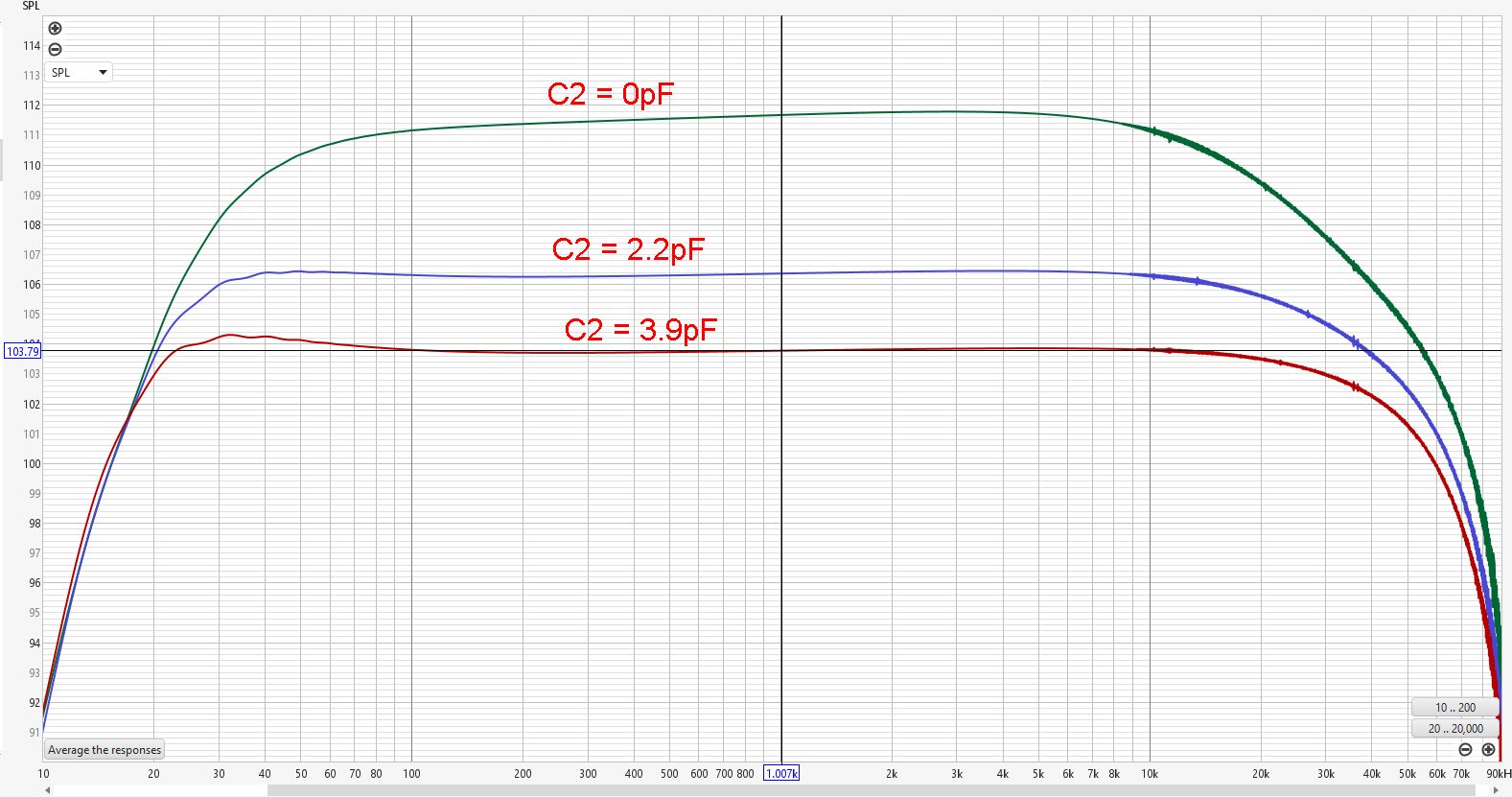
Frequency Response Chart of the KM84 circuit as a function of C2. (Ignore the SPL reading. Chart has been set to SPL only to allow alignment in the next chart.)
From this chart, we can read how the gain is affected by C2. But we can also see the low-end and high-end roll-offs being affected. This is more clearly shown when we align the plots in the next picture.

Aligned Frequency Response Charts of the KM84 as a function of C2. Aligned at 1 kHz.
As we can see, when increasing the value of C2, the output impedance of the JFET amplifier decreases, extending the bandwidth of the circuit. At the high end, you’ll get a simple RC low-pass filter if the circuit is capacitively loaded. At the lower frequencies, things are slightly more complicated: with a low output impedance from the JFET stage, a resonant bump in the 30-40Hz starts to emerge. This bump may or may not be acceptable, depending on your taste and the capsule’s low-frequency response. It compensates for the natural roll-off of the capsule, but in combination with the proximity effect, it might make the microphone sound too bass-heavy. It’s just something to be aware of when you want to change the value of C2 for whatever reason. The LF bump and roll-off also depend on the transformer chosen. So for each combination of JFET, C2, C4, and transformer, you’ll want to figure out what combination works out best for you.
C2 and how it affects Harmonic Distortion
By changing the value of C2, and thus the amount of feedback around the JFET, it will be clear that we also influence the THD of the JFET. That is how feedback works around amplifiers with not-so-very-low THD and an Open-Loop gain that is (much) larger than the Closed-Loop gain. But as said earlier, C2 also affects the output impedance of the JFET amplifier. And THD, mostly odd-order harmonics, of a transformer is greatly affected by the impedance of the driving stage. And just as with the LF bump, this could be acceptable, or even desired. Or it could become too much and objectionable. It all depends on your taste and on what instrument you are going to use the microphone. I’m not a musician or recording engineer myself, but allegedly some musicians make good use of overdriving a transformer-coupled microphone as an artistic effect by leaning in towards the microphone to get the intended overdrive distortion effect.
From the same set of FR measurement data shown in the previous paragraph, we can take the Harmonic Distortion content as a function of C2 and frequency. That’s a nice feature of REW: it does not only capture amplitude and phase as a function of frequency but a.o. also Harmonic Distortion. I’ve exported these data to Excel to capture the Distortion plots in one graph, separately for the H2 and H3 harmonics, which are the dominant harmonics. I’m not sure at which input signal amplitude I took these measurements, but I think they were taken at 100mV RMS, which equals ~114 dBSPL.
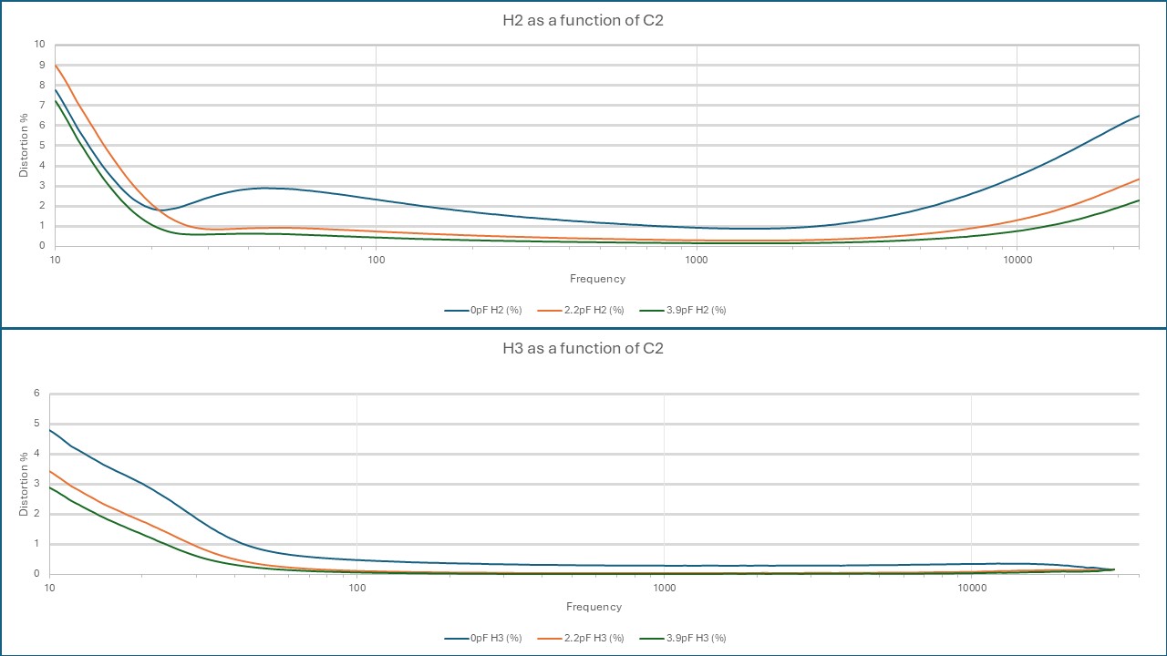
2nd and 3d Harmonic Distortions as a function of C2.
It is immediately clear from the graphs that C2 mainly affects transformer-generated H3 at low frequencies and H2 at high frequencies in combination with a capacitive load. Several percent of even Harmonic Distortion at high frequencies may not always be audible as a change of tonality because they end up in the area where the ear becomes increasingly insensitive, but along with 2nd Harmonic Distortion come much more objectionable intermodulation products. To complete the non-linear distortion picture, I decided to also measure the Difference Frequency Distortion with equal amplitude 6 and 9 kHz signals, resulting in a 3 kHz difference tone in the area where our ear is the most sensitive. I measured with and without 22nF caps on the microphone output, which are often added as RFI suppression. The Auditory Masking Plot below suggests that a frequency one octave below a fundamental tone playing at ~100 dB, can be heard even when it’s ~70-80 dB below the fundamental. With a fundamental at 6 kHz and a difference tone at 3 kHz, I would assume it can be heard even further below the fundamental. But let’s for now assume 70-80 dB is the threshold.
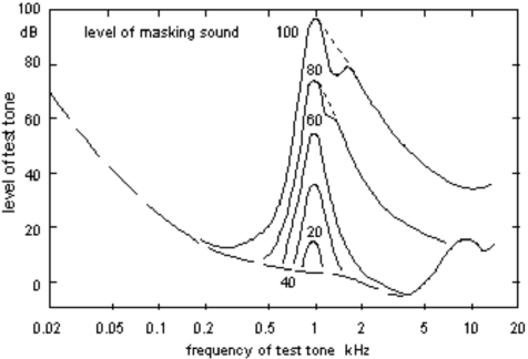
Auditory masking of the human ear.
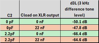
Difference Frequency Distortion measurements of the KM84 as a function of C2 and capacitive load.
The measurements reveal that even with a “decent” 2.2pF feedback capacitor, the DFD products might become audible under controlled circumstances and using sine waves as test signals. But when recording musical content, neither of these will be the case and under practical circumstances, this distortion is less audible than the Auditory Masking curves would suggest. But we’d better stay on the safe side if it can be done within reason. Without the feedback capacitor C2, the DFD products rise significantly by another ~16 dB. Unless you want to use this DFD distortion as an artistic effect, it might become objectionable.
The conclusion we can draw from all this is that it is not very desirable to leave out C2 completely. Already with a few pF we still have an acceptable gain, while the linear and non-linear distortions are reduced considerably. C2 should only be removed if one wants to use the resulting distortions as an artistic effect.
C4 and how it affects low-end Frequency Response and THD
Another important capacitor in the KM84 design is the coupling capacitor C4. It acts as a DC-blocking capacitor between the JFET Drain and the transformer primary. As we all know, transformers cannot handle DC and even if they could, the JFET stage cannot supply the DC that would flow through the transformer. So obviously, we need a coupling capacitor here. We should just give it a sufficiently high value as is common practice in audio designs, and we’re good to go, aren’t we?
No…
Bigger isn’t always better. Why? Because the transformer throws a spanner in the works and simply because you don’t want subsonic content to enter the signal path. There are two main reasons why you want to block sub-sonic signals:
- Subsonic frequencies as such may not be audible, but they will create audible intermodulation products.
- Subsonic frequencies can easily upset your transformer and saturate the core, which also causes distortions at higher frequencies.
So intuitively, there must be an ideal value for C4 that minimizes the issues described above but at the same time will also maximize the low-end bandwidth, preferably down to 20 Hz. Let’s see how we can get there. For the sake of understanding, I will first present a simplified representation of the transformer circuit, depicted below. Z_out represents the output impedance of the JFET amplifier stage, C4 is the coupling capacitor, L1 is the inductance of the primary side of the transformer, and Z-load is the impedance of the mic preamp, reflected through the transformer. In this circuit we immediately recognize a damped resonant LC circuit, but at the same time a 2nd-order LC high-pass filter as we know it from loudspeaker crossover filters. However, if C4 becomes sufficiently large and has an impedance much below Z-out, the circuit simplifies to a 1st-order RL high-pass filter. This is exactly what we see when stepping the capacitor from 10 nF to 100 μF in powers of 10, which is plotted next to the schematic.

With C4 being 10 nF and 100 nF respectively, we can see a resonant bump popping up (green and blue lines) and dropping off at 12 dB/oct below the resonant peak. This peak with low C4 values is not surprising, because the Quality Factor of the RCL resonant circuit is inversely proportional to the square root of L/C. So a lower C means a higher Q and therefore a higher resonant peak. If we want to use a smaller coupling capacitor as a low-cut filter, we have to add more damping to the circuit to prevent this bump. This is exactly what I’ve done in the low-cut filters of the KM84+ and KM84++. The same applies if we design an impedance converter circuit with a very low output impedance, which would also result in a high Q resonant peak. Due to the lack of a suitable transformer for the KM84++, which has a low output impedance JFET amplifier, I had to add additional damping in the circuit to prevent the bump.
At the other end of the spectrum, with C4 increased to 10 uF and 100 uF, we can see that the circuit has effectively changed to a 1st-order RL high-pass filter (cyan and magenta lines), sloping with less than 6 dB/oct . We observe now that the low-end output level starts dropping off at a much higher frequency than at a lower capacitance of 1 μF. From all these plots, it becomes quite obvious that there is an ideal value for C4 if we want to obtain a more or less flat response. This point can be deduced from the -3 dB cutoff points of the RL high-pass and the LC high-pass filters. Where they coincide, you have found the ideal capacitance value: any larger and the RL high-pass governs the Frequency Response, and any lower and you’ll get that bump and reduced bandwidth.
With the RL cut-off frequency being equal to fc=R/2πL and of the LC circuit being fc=1/2π√LC , we can derive the formula for the ideal capacitor value by equating both formulas. This yields C=L/R2 . Suppose we’re using the ASTDS T8 transformer and a standard KM84 circuit, we have L = 58H and R =7820Ω + 220Ω = 8040Ω (output impedance of the JFET + transformer DC resistance). This yields a capacitance of 0.9 μF. That is really close to the 1 μF in the original KM84 circuit…😊. With this capacitor, the calculated low-end cut-off equals 21 Hz. Nice! This proves we have a well-engineered circuit where the JFET, C2, C4, and the transformer are well-matched!
The above reasoning to arrive at an ideal value for C4 assumes a transformer that is well-matched to the output impedance of the JFET amplifier. If that is not the case, e.g. if you drive a transformer with a low-impedance output, you get a resonant peak that can be unacceptable. The same trick that I applied to flatten the curve when a small low-cut filter capacitor is used, can be used to flatten the frequency response when a low driver output impedance causes a resonant bump. As said before, this is further described in the KM84++ circuit.
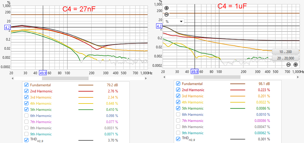
Now let’s have a look at how the coupling capacitor affects THD. By this, I explicitly do not mean the distortion of the capacitor itself, but the THD increase resulting from the rising impedance of the capacitor at low frequencies. But why would THD increase, you might ask? This has to do with the fact that transformers cause more distortion when driven from a high-impedance source. I will not go into the background of this phenomenon here, but let’s take this for granted now. Let’s see what happens when we choose 27 nF and 1 uF coupling capacitors. The graphs were taken with 100 mV input signal to the head-amp circuit (KM84++ in this case), which would equal a sound of ~105 – 120 dBSPL, depending on the capsule sensitivity. With a 1 uF coupling cap, we can see several % of distortion at the lowest frequencies, which btw is not likely to be audible (See this article here). Only under controlled circumstances and with sustained tones, the values listed in Table 2 in the mentioned article would suggest that these distortions are just audible. With a 27nF capacitor, which one could use as a low-cut filter, peak distortions move to higher frequencies, where the threshold of audibility decreases. So not only will we have a resonant bump when choosing a smaller coupling capacitor, but also much more (potentially) audible Harmonic Distortion. Fortunately, though, the trick that I use to tame the resonant bump will also lower THD significantly, so I would not rule out using a small coupling capacitor as Low-Cut filter, but a capacitor at or around the previously derived optimum value would yield lower THD.
RFI Sensitivity
Unfortunately, the KM84 is notorious for being sensitive to Radio Frequency Interference, especially from cell phones. Of course, it was never designed to be compatible with cell phone interference because in the 1960s, when the KM84 was designed, there were no cell phones. In this thread on GroupDIY, you can read all about it. I designed an RFI filter concept that can be universally applied in many microphone circuits and effectively reduces RFI sensitivity to a level where it no longer is an issue. The 22nF capacitors often found on microphone outputs are not always effective against cell phone interference, especially if the caps are wired components with high parasitic inductance and, hence, low resonant frequency. You can read more here about how this filter was designed and works.
The AM demodulation of the TDMA cell phone signal in the JFET stage can be simulated in LTspice. The schematic used in the simulations is depicted below. L1, L2, and L3 are beads that I inserted to explore how they would affect RFI sensitivity in this circuit. I will confine myself here to the variations in L1 (or any other impedance for that matter), the simulation results of which are plotted below the schematic. Note: The signal amplitudes shown have no relation to actual cell phone RF interference levels. The injected 500MHz/100mVp signal is only for demonstration of the AM demodulation effect.
The first set of plots depicted below shows the AM-demodulated signal at the circuit output without impedance L1 inserted (Left) and when a Murata BLM18HD102SN1 bead is inserted (Right). It would suggest a ~60dB improvement, but in reality, I measured a ~12dB reduction of the demodulated signal in a practical circuit. Still interesting when combined with another filter on the XLR output. The second combined picture shows what happens if we replace L1 with a 470R resistor and what if we completely remove C5. Thanks to the 7:1 transformer output, the resistor will only very slightly attenuate the signal and add negligible noise, so it could serve as a good alternative for a bead. More on this in the KM84++ description here. The last picture shows the detrimental effect of removing the feedback capacitor, which is C5 in the simulation schematic. I did not actually measure the differences on a KM84 circuit, but the sim suggests that this is another reason for keeping the feedback capacitor in.
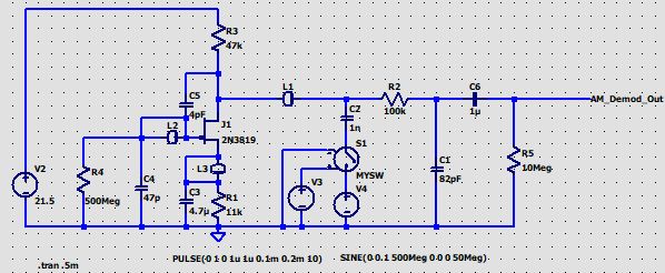

Left: no RFI suppression. The blue trace is the injected 500 MHz RF signal. Right: L1 bead inserted.

Left: L1 is a 470R resistor. Right: C5 was removed from the circuit.
Conclusions
Summing up the observations and (obvious) conclusions:
- At first glance, the KM84 circuit seems simple, but because of this simplicity, it also has many pitfalls and limitations. Yet, Neumann managed to make a well-thought-out and well-balanced design.
- This doesn’t mean there are no possibilities for further improvement, but they are mostly limited to noise reduction and RFI suppression. This is exactly what I’ve done in my KM84+ and KM84++ designs.
- If you want to replicate the KM84 circuit, you may find that you’ll have to tweak some component values, in particular C2 and maybe C4 to maintain the same well-balanced circuit properties as the original KM84 circuit. The methods to determine the ideal values have been described.