For the Audio Analyzer Microphone Preamp, I had the following set of requirements in mind:
- Lowest possible noise and distortion (of course). Ideally, the Equivalent Input Noise (EIN) of the Preamp plus Line Input amplifier should be lower than the noise of a 150 Ohm resistor, which is often used as a reference when measuring the EIN of a preamp or ADC. Over a 20Hz–20kHz bandwidth and at 25 °C ambient temperature, the RMS noise of a 150 Ohm resistor equals 222.1 nV, or approximately -131 dBu (unweighted). Measurements by Julian Krause (See here) suggested that the UMC202HD does not quite reach this performance and would end somewhere around -127dBu (unweighted). My measurements on the UMC202HD support that.
- Preferably flat within 0.1 dB from 20 Hz to 20 kHz, even at the highest gain setting. But +/- 0.5 dB would still be acceptable, as this is still practically inaudible. Moreover, the transfer function of the complete system can be calibrated out in REW.
- The output of the preamp connects to the Line-Input, which has a differential input with 200 mV sensitivity at -3 dBFs. So it will have a differential output.
- It shall have fixed gain settings for 2mV, 20mV, 200mV and 5V input levels at -3dBFs. And a variable gain with a multiturn potmeter. With the 200 mV sensitivity of the Line-Input, this sets the required gain to 100, 10, 1, and 0.04, respectively. The variable gain will be 200 max.
- There shall be a switchable 48V phantom power supply.
- It must have some level of overvoltage protection on the input, which should be able to handle surge currents that occur when shorting an input to ground when phantom power is engaged. The protection circuit should not increase noise or distortion.
- Selectable input impedances: 1k, 3k and 8k (+/- 10%).
- RF filter on the input.
- A CMRR that is as high as possible, which I wanted to achieve by using 0.1% resistors and 1% or 2% ceramic capacitors and by matching components of the inverting and non-inverting input sections.
As this is a one-off product and I wanted to circumvent trim pots and trim caps, this is one of the rare occasions that I allowed myself to use hand-picked and matched components. By doing so, I was able to obtain good CMRR values. The circuit I finally came up with is shown below.
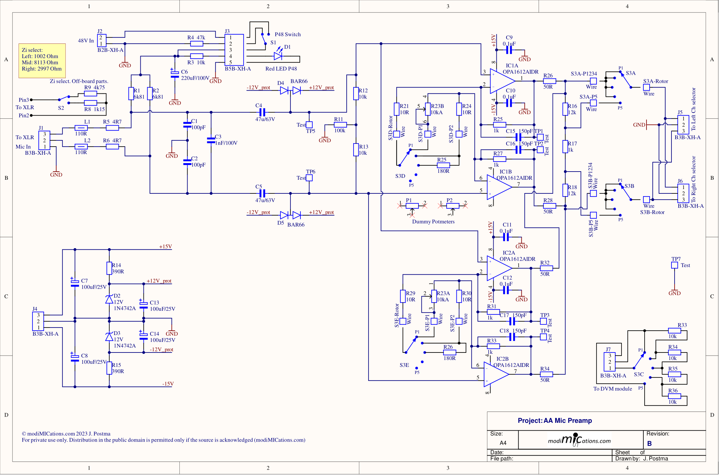
Circuit diagram of the Audio Analyzer Mic Preamp
Below, you see a picture of the preamp module in the Audio Analyzer.
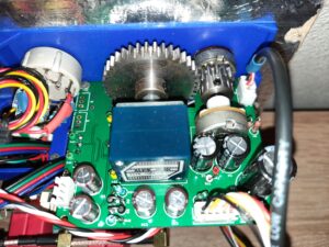
Now you may wonder what those gears are doing there. And perhaps you want to know a little more about the mic preamp design process and how I utilized LTspice to simulate and optimize the noise performance. If so, read on to learn more about the Microphone Preamp design.
Microphone Preamp design contemplations: which circuit topology to choose?
When I set out and started the mic preamp design, the first question was which topology I should choose. A standard low-noise microphone preamp circuit with PNP BJT or CFP input, as commonly found in many mixing desks, would probably have noise specs that would satisfy my requirements. An example of such a circuit can be found on the Elliot Sound Products site. For a flat frequency response down to 20Hz, this circuit requires a very large capacitor in series with the gain-setting resistor (C1 in Rod Elliot’s circuit). Or one would have to increase the gain-setting resistors, which would compromise noise performance. Moreover, as the capacitance and ESR of electrolytic caps depend on time and temperature, fixed gain settings may lose accuracy over time. But perhaps the cap can be left out if we trim the circuit or when we use a servo loop, something I did not explore any further. Finally, I was also afraid the THD would be worse compared to an Op-Amp solution. All in all, I found the classic mic preamp circuit would have too many uncertainties and would probably need some design iteration loops, which I hoped to avoid. So I decided to opt for an Op-Amp circuit with state-of-the-art low-noise Op-Amps or with a dedicated preamp IC.
EDIT 2025-08-31: For quite some time, I have had another mic preamp installed in the Audio Analyzer, based on the THAT1580 preamp IC. It has excellent performance, even slightly better than the design described further down. I had issues with the bulky, cheap Chinese rotary switch, used for Gain selection. I then exchanged it for a relay board, but the wiring became too long and the amplifier became unstable. I then decided to abandon the original circuit and design a whole new preamp board, but without the bulky multi-turn anti-log potmeter construction. Without much more explanation, you’ll find the schematic depicted below.
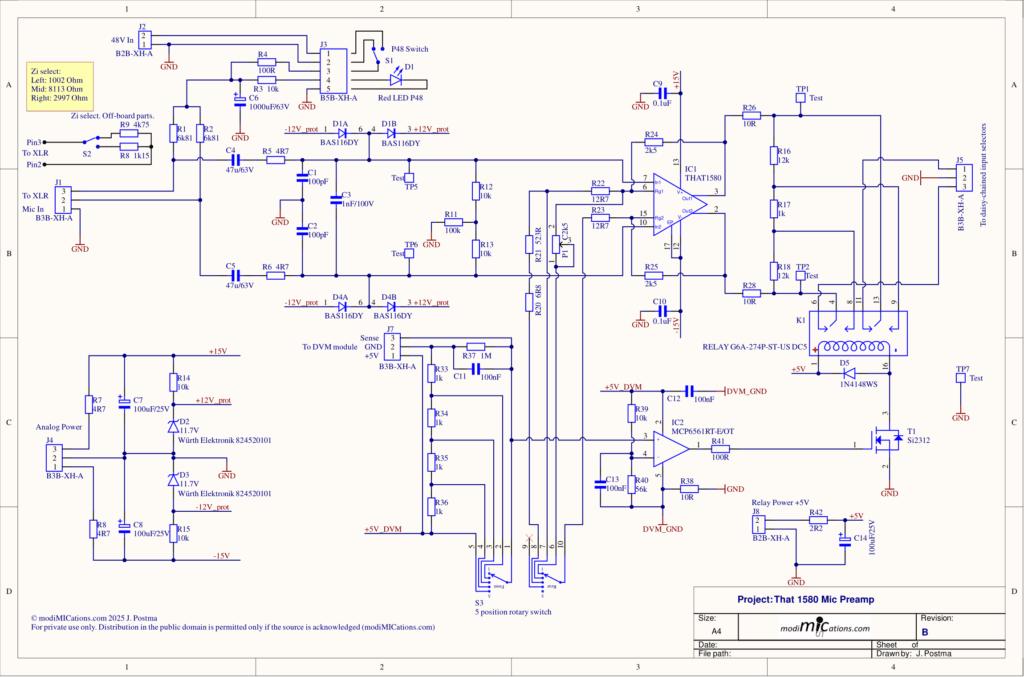
First iteration of the Microphone Preamp
There are several well-known Mic Preamp ICs available on the market, e.g. the obsolete SSM2017 from AD, TI’s INA217, or TI’s new INA849. They would seem to make designing a preamp a breeze, but they all have in common that the output is single-ended, which is not what I needed. What I needed was a differential output that interfaces to the differential Line-Input stage following the Mic Preamp. The first half of a complete Instrumentation Amplifier (INA) circuit, so without the differential-to-SE output stage, would satisfy. Instead of using a dedicated preamp IC, I decided to design a circuit myself utilizing the ultra-low-noise OPA1612 dual Op-Amp from TI. The circuit was simulated in LTspice to predict and optimize its noise performance and is depicted below. A nice introduction to LTspice noise simulations can be found here, by the way.
Not all parts are equally relevant to the noise simulations, but have been added anyway. Here’s the LTspice circuit.
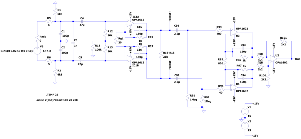
First iteration of the Mic Preamp circuit for noise simulations.
In short, these are the functions of the components in the diagram:
- IC1A and IC1B are the actual differential amplifier. U1, U2 and U3 consitute the Line-Input amplifier.
- R1 and R2 are the phantom power supply resistors. These are AC coupled to the signal ground.
- Rmic is the source impedance. To simulate the noise performance of the circuit alone, this should be kept to 0 Ohm.
- V3 is the signal source. V(inoise) is the input-referred noise from this source and will be simulated.
- C4 and C5 are the input coupling capacitors. I chose bipolar types because Cyril Bateman’s measurements on capacitor distortions suggest that bipolar elcaps produce less distortion compared to polar types.
- R5 and R6 reduce the potentially destructive input surge current through C4 and C5 when Phantom power is engaged and an input terminal is shorted to ground (“The Phantom Menace”, see this AES paper by the THAT Corporation). The value includes the small series resistance of the ferrite beads (not shown).
- R11, R12 and R13 provide an input bias current path to the OPA1612 inputs. R12 and R13 resistor values are quite high compared to what you see in e.g. INA217 circuits you’ll find online. Generally speaking, they are connected to the ground, whereas in this circuit, R11 was added. It was purposely done this way to improve CMRR when there’s an impedance imbalance in the signal source or signal source wiring. It will also help to extend the frequency bandwidth at the bottom end, without having to resort to large-value capacitors for C4 and C5. Large C4 and C5 values would also require more robust input protection diodes (not shown in the LTspice circuit, btw). A low microphone termination resistance was achieved by adding a resistor between the input terminals before the input coupling caps. (These are R8 and R9 in the Mic Preamp circuit diagram. Not shown in the LTspice circuit diagram.)
- C1, C2 and C3 constitute an RF filter, together with the ferrite beads L1 and L2 from the AA Mic Preamp circuit diagram and input resistors R5 and R6. For the best RF common mode suppression, C1 and C2 should be wired to the chassis ground, but they are connected to signal ground on the PCB. On 2nd thought, I think it would have been best if I had placed this filter, together with a common-mode choke, on the XLR connector with a short connection to the chassis ground.
- R25 and R27 are the feedback resistors of the differential amplifier circuit. Together with Rg1, they set the gain. In the LTspice simulation, Rg1 equals R21 + R24 on the Mic Preamp circuit diagram. The gain equation for this circuit equals G = 1+ (R25 +R27)/Rg1 = 101. Slightly higher than the 100X gain as mentioned in the requirements, but this is not a problem. For the lowest noise, the resistors should be chosen as low as possible. But there are some limitations. First of all, distortion would rise if resistor values were further reduced. Secondly, I was afraid the contact resistance of the rather poor-quality rotary switch I had decided to use would affect the gain stability.
Now let’s see how well the circuit performs in a noise simulation, where I plotted the input-referred noise EIN across the audio band.

EIN plot of the above circuit. EIN (unweighted) equals 265.59nV, which equals -129.3 dBu.
With an EIN of -129.3 dBu, we can conclude that it is not at the desired -131 dBu level yet, so let’s explore how we can further improve the noise level. To do that, we first need to know what the main sources of the noise are, other than the Op-Amps. We take the OPA1612 Op-Amps as a given because, AFAIK, there are no other significantly better, affordable types available on the market.
If you did not already know that the key noise-contributing resistors in this circuit are the gain-setting resistor Rg1 between IC1A and IC1B and the input resistances, you could have learned this from LTspice noise simulations. There are several ways of using LTspice to find the noise sources and use the LTspice features to improve the circuit. The first method that I typically use when the circuit is not too complex, is to just left-click all resistors after the simulation has run, which displays their noise contribution to the output signal. The resulting plot is shown below.

Circuit noise simulation showing the individual contributions of all the resistors and the complete circuit noise.
The upper green trace is the total output noise voltage V(onoise). The red trace is the most dominant noise contribution from the resistors, which in this case is from the Gain resistor Rg1. We see there’s a wide gap between the Rg1 trace and the total noise, so apparently the Op-Amps are by a distance the dominant factor. Hence, further reducing the resistor values doesn’t make much sense and will only load the Op-Amps more, thus potentially increasing their THD without any other benefit. Another reason to not reduce Rg1 any further is that you don’t want the contact resistance of the gain selection switch to noticeably affect the gain. As a matter of fact, the cheap Aliexpress rotary switch I used did affect the gain. I had to apply some contact spray to get a stable gain.
Another method of finding the main noise-contributing resistors is to make all resistors noiseless by adding the word “noiseless” as a suffix to the resistor value. When simulating the circuit with noiseless resistors, we will only see the contributions from the active parts, which are the Op-Amps in this circuit. The resulting noise plot is shown below.

Noise contribution of the Op-Amps, all resistors defined as “noiseless”. EIN equals 246.71 nV, or -129.9 dBu.
Again, we can conclude the Op-Amps are the main noise contributors because the noise is only marginally lower compared to the original circuit with the noisy resistors. And when we restore Rg1 to a noisy 20 Ohm resistor, we’ll find 259.48 nV EIN from the simulation, which is very, very close to the 265.59 nV we found earlier.
Second iteration of the Microphone Preamp (noise optimized)
Now that we know that the theoretical limit of this circuit is -129.9 dBu and that reducing the resistance values further makes no sense, we have to come up with a trick to achieve a lower noise figure. Let’s see what happens if we parallel two of the OPA1612 INA input stages. This will complicate the gain adjustment circuit as we will see later, especially if we want a continuously variable gain with a multiturn potmeter. But let’s give it a shot… The circuit will now look like pictured below. R26, R28, R32 and R34 have been added as summing resistors. The differential input amplifier dominates the EIN, so when paralleling two of these amps, we should be getting an almost 3 dBu better noise level.
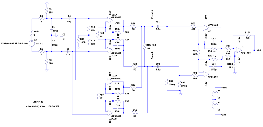
Second iteration of the Modified Mic Preamp + Line Input amplifiers;. Now with two parallel differential input amplifiers.

EIN plot of the above circuit. EIN (unweighted) is 192.61nV, which equals -132.1 dBu.
Now we’re getting somewhere… The noise level has decreased by 2.8 dBu, exactly as expected. This circuit does fullfill the requirement of a noise level below -131 dBu, so I decided to use it in my final design. When I determined the actual EIN of the completed circuit, I measured -131.1 dBu. Not exactly the same as the simulation predicted, but pretty close and good enough.
The mysterious gears explained…
By putting two differential amplifiers in parallel, I created a big challenge for myself concerning the variable gain potentiometer. I wanted it to be a multiturn potmeter, so it would be easy to accurately adjust the gain. Secondly, to avoid the sharp gain rise at the end of the potmeter travel, it should be an anti-log potmeter. And as we have to adjust the gain of two INAs simultaneously, it should also be a ganged, dual potmeter. Now, tell me: where on this earth can one buy such a dual, ganged anti-log multiturn potmeter…? Unobtainable, I’m afraid. And if it were commercially available somewhere, then it would be horribly expensive. Instead of throwing in the towel and going for the single INA circuit, I thought it would be fun to build such a potmeter myself. How? When you take a close look at the pictures below, most of it will become clear.
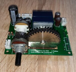
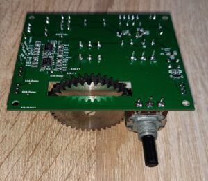
The DIY Vernier reduction, including the reversal of the direction of rotation on the ALPS potmeter.
First, to obtain an anti-log potmeter, I had to reverse the rotational direction of a regular logarithmic potmeter. This was realized through the gears you see in the picture. A vernier reduction was realized by making the gear on the potmeter larger than the one on the dial axis. A vernier reduction would only make sense if you have a potmeter with high resolution, such as the 27mm diameter ALPS RK271 series. I used the logarithmic stereo ALPS RK27112 10k model. Next to this potmeter you can see two small 16mm potentiometers in the photo. The one with the white face-plate is still intact and its long axis extends through the Audio Analyzer front panel. The axis sticks through the potmeter housing located on the board edge. The innards of this potentiometer have been removed, so that the shaft of the other potmeter can protrude through it from back to front. For this potmeter, you’ll want a type of which the backside contains a hole of the same diameter as the axis, such as the Omeg PC16BU. In this way, it will serve as mechanical support to the gear axis. The gears are a Reely type 231797, 40-teeth gear on the ALPS potmeter and a Reely type 231762, 15-teeth gear on the dial axis. This gives a 2.67 times vernier reduction, changing the 300° rotational angle of the potmeter into 800° (Or 2.2 full turns). More turns would make gain adjustment even easier, but this, together with the anti-log feature, made gain adjustments already way easier than would ever be possible with the tiny gain pots on the UMC202HD, or any mixing desk gain potmeter for that matter. The whole construction, together with the large gain adjustment knob, gave it a very professional feel with a smooth operation, and the right amount of resistance to my experience. A Bourns multiturn potentiometer, on the other hand, turns so smoothly that it will turn again slightly as soon as you release the dial. Not so with this potmeter. Like it or not, the gain adjustment was smooth and far easier to adjust than the UMC202HD gain pot.
Circuit improvements or modifications
Of course, nothing is perfect. Or maybe you find the circuit too complex. So here are some ideas for improvements or adjustments you might want to make to this circuit.
- Use a commercially available Vernier reduction, such as this one. But I’m afraid it does not reverse the direction of rotation. I could not find a commercially available Vernier reduction that reverses the direction. But if you opt for a single differential amplifier solution and use a single anti-log potmeter, then you can use a regular Vernier reduction without direction reversal. I think I would prefer such a solution over a regular multiturn potmeter.
- THAT Corporation published some design ideas that should prevent microphone preamps from being destroyed by surges caused by, among others, shorting the inputs of a phantom-powered microphone preamp to signal ground. These ideas were published in two AES papers, here and here. At the time I designed the preamp, I did not know these papers, but I just mixed and merged some of my ideas with what I found in other designs. Perhaps you want to increase R5 and R6 to 10 Ohm, use bigger protection diodes (e.g. 1N4004 or similar) and add 1N4148 diodes from the inputs to the Gain resistor (D5 and D6 in Fig. 24 of the 2nd THAT paper). The BAR66 diodes should be more robust compared to the 1N4148 diodes you see in many other Mic Preamp circuits, but they may still not be able to handle the surge currents, although they are intended to be used in such protection circuits. In any case, I would leave the +/-12V clamping circuit around D2, D3, C13 and C14 as is. By clamping below the supply voltage of the Op-Amps, currents through the Op-Amp input protection circuits are avoided. And the elcaps absorb energy peaks that the zeners may not be able to handle. Alternatively, TVS diodes could be used, but I think a zener + elcap will work just as well. And by biassing the zeners, leakage currents through the zeners which might cause some distortion, are avoided.
- Mounting the RF filter C1, C2 and C3 together with a common mode choke on the XLR connector might yield better RF attenuation.
- Instead of using a rotary switch to adjust the gain, it is better to use signal relays with gold-plated contacts. Good multi-deck rotary switches are very expensive. Relays might be cheaper and, when mounted on the PCBA, will avoid the noise-sensitive wire clutter between the rotary switch and the PCBA. The rotary switch can be a cheap 6-position, 2-pole switch like this one. One of the poles can be used for the DVM, and the other pole to power the relays that switch the gain resistors. Good relays for this purpose are special Low-Signal types, specified for low minimum currents (typically 10 µA), and should ideally be with Bifurcated cross-bar contacts (i.e. double contacts). Such relays include the Kemet UC2/UD2 series (used in AP analyzers), the Kemet EA2/EB2 series, and the Omron G5V and G6K series. The G5V offers the lowest specified contact resistance if you opt for the Normal version, but the EA2/EB2 series has the longest specified lifetime and would be my preference. But there are other, good signal relays around to choose from. See the table below, which summarizes the main specifications for this application of the aforementioned types.
