Let’s start by listing the requirements. The output buffer should have the following features:
- Two switchable, adjustable output levels of 1 V and 10 V Single-Ended or 2V/20V differential at -3 dBFs DAC output level.
- Ideally, in a loop-back test, a flat frequency response within +/- 0.1 dB. But at least it should be better than +/- 0.5 dB.
- Level adjustment using a 10-turn potmeter.
- Single-Ended Output Impedance is selectable between 50 Ω and 150 Ω.
- Output is protected against short circuits, overloads, and overvoltage spikes (e.g. due to disconnecting transformers).
- True RMS output to the DVM module.
- Output to headphone amplifier.
- And, of course, low noise and low distortion. However, the output noise is spoiled by the lack of a decent LPF in the Behringer, so even if I used an extremely low-noise Op-Amp, it wouldn’t help much. And I did not want to add another LPF stage, further increasing complexity and possibly some extra distortion.
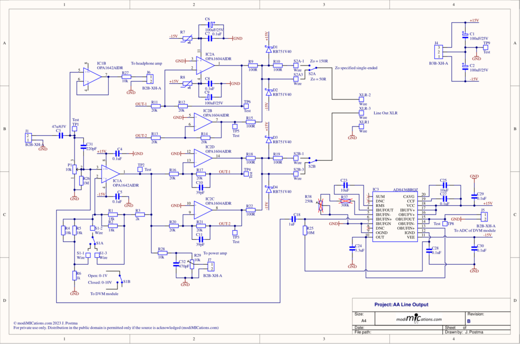
The resulting circuit is depicted below.

Audio Analyzer Line-Ouput Stage Circuit Diagram.
The Single-Ended input signal comes from the UMC202HD output DAC buffer, as described in this article. This signal is available on the potmeters and switches riser board in the UMC202HD. Upon entering the Line-Output circuit, the signal is routed to the headphone amp buffer IC1B and potmeter P1. P1 is a 10-turn Bourns multi-turn potmeter. In hindsight, I’m not too happy with it. As it is wire-wound, it has an inductance, which causes high-end roll-off. To compensate for that, I added C31, but you still won’t get a flat frequency response. I played with the value of C31 until I got a response with a maximum high-end tilt or roll-off of less than 0.5 dB over the entire potmeter range. Perhaps I should have taken an ALPS RK271 series potmeter and added a Vernier reduction. Or use a digital potmeter. But hey, I wanted to keep it simple… So I’ll keep things like they are.
Switch S1A adjusts the IC1A gain and switches between 1 V and 10 V range. The output of this amplifier goes to the external Power Amplifier which can be used to drive passive speakers in an audio setup or to do Thieleme-Small parameter measurements on drivers. And of course, this signal is fed to the output buffer stage around IC2.
The positive and negative sections of the Output Buffer stage consist of two Op-Amps connected in parallel for more output power. Perhaps a bit over the top, but I protected IC2 against overcurrents through 50 mA Resettable Fuses in the power lines. The outputs should be short-circuit proof, but I didn’t want to take chances. Diodes D1, D2, D3, and D4 protect the outputs against inductive spikes that can occur when disconnecting a powered transformer under test. S2 switches between 50 and 150 Ω output impedance (Single-Ended).
IC3 is an AC-to-True RMS converter that measures the output level and feeds the DC signal to the ADC of the DVM module. It measures the unloaded output voltage of the Output Buffer. This was the easiest way to do it, but if you want to know the output voltage under load, you’ll not only connect the output to the DUT, but also to one of the inputs and read the actual voltage on the DVM channel of that input. In this module, I left out the LPF filter on the True RMS converter input. I guess I should have done that because I sometimes get the idea that out-of-band noise gives a measurement error.
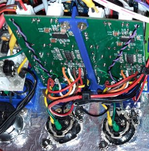
I don’t have a good picture of the completed module. The one below shows the bottom side of the PCBA and all the cable clutter I already spoke about earlier. But I’ll repeat myself here: if I were to design and build one again, I wouldn’t have done it this way.

Circuit modifications
In the circuit description, I already mentioned some possible improvements or possible alternative solutions. Here’s a list of what I can think of right now.
- RK271 potmeter with Vernier reduction instead of a multiturn potmeter.
- DRV134 or OPA1632 output stage. Disadvantages: DRV134 has more HD and OPA1632 does not have a rail-to-rail output voltage. I don’t expect it to be able to reach an output RMS level of 10 V SE or 20 V differential. OPA1632 is limited to +/-15 V supply rails.
- LPF before True RMS converter input. But if the DAC would have had a decent LPF on the output, this may not even be necessary.
- Connect the True RMS converter input to the buffer output, after the output series resistors to measure the true output voltage. You’ll have to introduce a voltage divider to keep the converter input within the desired range when the 0-10 V output voltage range has been selected. But when using some solid-state switches controlled by S1B, this shouldn’t be too difficult.