Introduction
As most are aware, many famous and popular products from Western brands are shamelessly copied by Chinese companies and sold through channels as Aliexpress, Temu, or Alibaba. One of these products is the Neumann KM184. It’s a popular SDC with very low self-noise (13 dBA), selling for ~1300 Euros a pair in the EU. On Aliexpress, the clones sell for ~340 – 400 Euros a pair. A significant difference. What you get for that money and how this clone compares to the original KM184 is discussed in this thread on GroupDIY. In that thread, you can find enthusiastic reviews of this clone. However, there was also a known case of a pair that was very noisy. I haven’t directly compared the original, the noisy, and the allegedly good clone microphones, but I did receive one of those noisy KM184 clone PCBAs for analysis from GroupDIY member RuudNL, and I can confirm it was quite noisy, indeed. Together with photos of a newer (or different?) KM184 clone PCBA, I was able to draw up the schematic, and I analyzed why RuudNL’s PCBA was so noisy. I will describe the results in this article. Huge thanks go out to members RuudNL and thecr4ne on GroupDIY for kindly providing the PCBA and the pictures. And of course, we have to thank MADON: They spent time and money dissecting and reverse engineering an expensive Neumann microphone, something no one in their right mind would do. And we should thank them for not applying potting material to their PCBA, like Neumann does, which greatly simplified reverse-engineering the circuit 😊. Before I delve into the schematic, a few disclaimers and notes:
• Although the MADON KM184 closely resembles the Neumann KM184 PCBA, they may have used different component values, types, or manufacturers for the parts. However, I don’t expect MADON to have made any conceptual changes to the circuit. Anyway, I’ve done my best to accurately draw up the schematic, but I cannot rule out the possibility of errors or the Neumann KM184 being slightly different.
• While I don’t believe it’s illegal to reverse engineer products, it is illegal to clone products and market them under the original brand name. If you decide to buy this MADON KM184 clone, then consider that you are supporting a multi-billion-dollar Mafia industry. The people behind these businesses don’t hesitate to physically intimidate and harass investigators who track down these illegal manufacturers. That this happens is not a myth but a fact. The company I work for has the necessary experience in this area.
The KM184 Clone PCBA
The picture below shows three different KM184 PCBAs: the top one is an original Neumann KM184, the middle one is the KM184 clone PCBA I got for investigation and repair, and the bottom one is likely a newer version of the KM184 clone. The bottom picture was kindly provided by GroupDIY member thecr4ne. It is quite obvious from the pictures that MADON attempted to make an exact 1:1 copy of the KM184, except for the conformal coating or potting material that Neumann applied. I used the reference designators visible in the bottom picture in the schematic displayed further down. Upon examining the PCBA under the microscope and drawing up the schematic, I noticed that the right terminal of C15 in the middle of the PCBA was not connected to Ground, as it should have been. C15 is the decoupling capacitor for the capsule bias voltage. I had hoped that restoring the ground connection would solve the noise issue, but it didn’t.
The left half of the PCBA is occupied by the impedance converter, of which Neumann covered most of it with conformal coating or potting material. They probably used black material instead of the more common translucent conformal coating to make reverse engineering more difficult. On the far left of the PCBA you can see an almost closed guard ring, which is also visible on the other side of the PCBA. The capsule bias generator, power supply components, and the output circuit components occupy the right half of the PCBA.
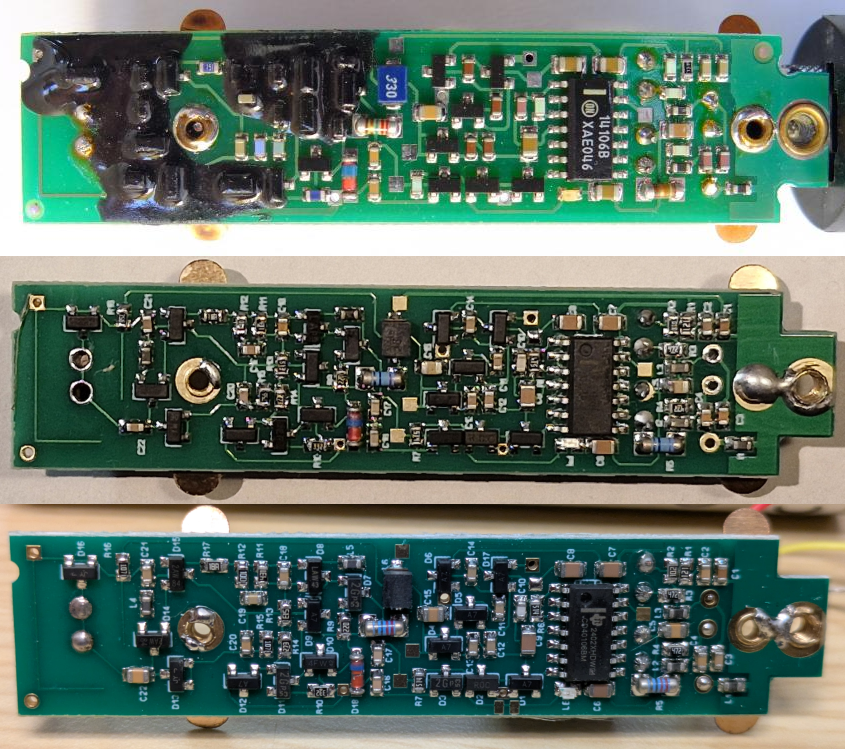
Neumann KM184 and clone PCBAs bottom sides with surface mount components.
Clone PCBA top side
Circuit description
Before describing the circuit, a note about the reference designators of the semiconductors. The MADON engineer who drew the circuit diagram decided to assign the prefix D to most of the semiconductors, while the prefix D is normally reserved for diodes only… This can be somewhat confusing. Therefore, whenever I refer to such a component, I will prefix the designator with the component type.
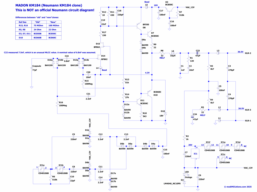
KM184 clone circuit diagram
The complete circuit consists of two main parts: the impedance converter, which includes JFETs D14 and D15, and BJTs D7, D8, D10, and D11. The other part is the power supply and capsule bias generator or charge pump circuit around IC1.
The impedance converter:
The impedance converter circuit has a single-ended output, so it drives only one of the XLR outputs. This is in contrast to a Schoeps circuit with a phase splitter. The advantage of this configuration is that it typically gives a better signal-to-noise ratio, although a phase splitter would double the output level. The reason is that a phase splitter always requires a resistor to obtain the inverted voltage that is not in a feedback loop. This resistor, typically a few kΩ, will add noise. A (minor) disadvantage of this type of single-ended design is that the outputs contain E-caps, which can potentially cause CMRR degradation when they do not perfectly match. And some claim they adversely affect the sound, which I can imagine will be the case when the value is too small or when Class 2 ceramic capacitors (X7R, X5R, Y5V etc.) are being used. They also have a finite lifespan, though good caps can last for ages. All these reasons may be more of a perceived drawback, but for me, they are the reasons to avoid E-caps in microphone output stages, especially because of the potential for CMRR degradation. But the Neumann KM184 sounds great, so who am I to say it’s not a good solution…?
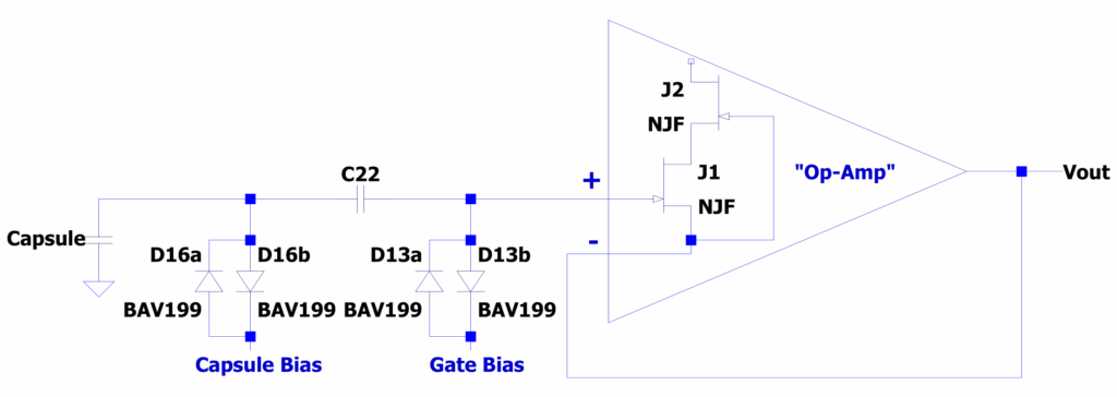
The impedance converter circuit is very similar to that of the TLM 103 and possibly other Neumann TLM circuits. If we follow the signal from the capsule, we see that the bias for the capsule and the gate of the JFET isn’t using the usual 1 GΩ resistors, but rather anti-parallel diodes fed with a bootstrapped voltage via Rx + Cx and Ry and Cy. This is an elegant way to eliminate expensive and/or large 1 GΩ resistors, while simultaneously achieving very low noise. This method has become particularly well-known on GroupDIY thanks to @MicUlli’s designs. A potential drawback is that LF peaking can occur if the bootstrapping circuits are not properly sized. The MADON KM184 I tested seems to suffer from this as well. More on that later.
The signal then reaches the gate of the first JFET via the DC blocking capacitor C22. The second JFET serves as a cascode. Interestingly, the drains of the JFETs are used as the source, and vice versa, likely because this was more convenient for the PCB layout. In principle, you can swap the drain and source when using fully symmetrical JFETs. The MADON PCBA uses BF862 JFETs, which are supposed to be symmetrical. These JFETs, famous for their low noise and high gm, were once manufactured by Philips/NXP but are now end-of-life. These must therefore be BF862 clones of unknown origin and quality. So I wouldn’t be surprised if Neumann uses a different JFET in their KM184, but I can’t verify that. In any case, whatever JFET is in there, the cascode arrangement of the JFETs significantly reduces the input capacitance of the circuit, as seen by the capsule, resulting in less signal attenuation of the capsule signal. This cascode also makes the JFET stage more linear and allows for the use of low-noise JFETs that often come with high input capacitance. The bias current of this stage is approximately 1.5 mA, which is much higher than Neumann’s KM84 and U87-like circuits. This, too, results in a more linear behavior and lower noise. The bias current from the JFETs then flows through output BJT D10, causing the output BJTs D7 and D10 to be differently biased. Without an AC signal, BJT D7 is mostly off and will only conduct with large signals and low load impedances. A kind of asymmetric class AB configuration, mostly operating in the Class A region.
The JFETs serve as the input of a differential amplifier in an otherwise fairly classically constructed amplifier with 0 dB closed-loop gain. The gate of the first JFET serves as the non-inverting (+) input of the differential amplifier. The drain, which in this circuit functions as the source, is the inverting (-) input and connects directly to the output of the amplifier stage. For those familiar with op-amp circuits, an equivalent circuit with an op-amp is shown below.
Via drain resistor R17, whose function I don’t quite understand, the signal ends up on R11, the compensation networks around it (R12, C19, and C18), and the base of BJT D8. BJT D8 is the Voltage Amplifier Stage (VAS), as we know it from a classic amplifier. The collector is loaded with a constant current source around BJT D11 to achieve a higher open-loop gain and lower the distortion.
The amplifier’s output signal is fed via R8, L6, and C23 to the non-inverting output (XLR pin 2). Edit: I first wrongly assumed it went to pin 3.
The inverting output (XLR pin 3) receives no signal and is only impedance-balanced via R5 and C24. As I noted earlier, I’m not entirely enthusiastic about this configuration, particularly because of the potential CMRR degradation when both output caps are not identical. Yet, when measured and compared to standard Schoeps circuits and my improved CMF (Sziklai pair) Schoeps output stage designs, the KM184 falls somewhere in between. At 50 Hz, it’s about 17 dB better than standard Schoeps, but lags the CMF Schoeps by 5 to 18 dB, depending on the circuit compared to. When shunting one of the output caps with 4.7uF to simulate a 10% mismatch between the E-caps, which is not uncommon for cheap brands, the KM184 still has the edge over the standard Schoeps, but the gap reduced to 12 dB. Assumingly, still quite good and usable, though there are conceivably better circuits. It depends entirely on the whole recording setup and the amount of EMI present, whether this is good enough.
I also did a comparative measurement of the RFI rejection, using my RF jammer circuit, and compared it to the Takstar CM-63, and some of my SDC designs. Despite the RF filters L1, L2, L3, C3, and C4, there was some measurable and audible interference, but not as much as in many other (budget) SDCs. The CM-63 and my SDCs were completely silent. For optimal filtering, this circuit layout on the PCB must be perfectly symmetrical and with RF design rules in mind, which is not the case. And perhaps the less-than-optimal RFI rejection is also due to the choice of the ferrite beads used: the beads on the MADON PCBA have an impedance peak around 100 MHz, while the beads I use peak around 700 MHz, which is in the GSM band where one can expect most RFI. Assumingly, the RFI is still quite acceptable, but then again, there are conceivably better circuits. And those better executions do not necessarily cost more: it’s just a matter of designing a proper PCB layout, with RF in mind.
Talking about RFI rejection, I find it surprising that the circuit ground connects to the mic tube through two spring tabs. When someone touches the mic tube, that person will act as an antenna and, due to bead L1, will inject an RF common-mode signal on the signal ground. I had expected the tabs to connect to the XLR-1 ground, so you’ll get a contiguous Farady shield of mic tube and XLR shield, of which the effectiveness is only deteriorated by the inductance of the XLR-1 “pig-tail” and pin inductance that are between the XLR cable shield and mic tube. Anyway, when testing the RFI rejection using my jammer and with the antenna held close to the mic body, I could not detect elevated RFI levels. So somehow, the KM184 solution does work, and it’s not as bad as I had assumed it would (or could) be.
I’d like to conclude this section with a note about R5 and R8. As you can see in the photo of the PCBA, these are MELF resistors. Assumingly, because they can handle high peak currents, such as those that can occur with hot swapping. Regular 0603 Thick Film, and possibly even 0805 would not be able to handle the high peak currents. Special pulse withstanding 0603 and 0805 resistors exist, which should be able to handle such peak currents, but Neumann chose MELF resistors instead.
Power supply and capsule bias generator:
The most remarkable aspect of the KM184 circuit, IMHO, is the power supply and the capsule bias generator. In terms of its power supply, the bias generator is “stacked” on top of the impedance converter circuit. This is the same idea as the Schoeps circuit, where the PNP output drivers are “stacked” on top of the impedance converter/phase splitter. This way, the supply current from one circuit is “reused” in the other. This can be useful and makes sense if your circuits, when connected in parallel, would consume more current than you could draw from the P48 phantom power. However, the KM184 only draws 3.5 mA, and would draw soapproximately 5 mA with the circuits in parallel. That’s well below the 10 mA that the P48 can supply according to the IEC standard. So I see no advantage here. In fact, by stacking them, the supply voltage per circuit is lower than what would be possible with a parallel connection. This unnecessarily limits the amplifier’s headroom, which in turn limits the maximum SPL. The charge pump circuit also becomes slightly more complex to create a negative voltage. In one of my designs, I generate the same negative voltage, but using three fewer components. The power supply circuit also becomes slightly more complex because two circuits now require their own stabilization circuits. These include BJT D3, C16, C17, and R7 for the amplifier, and Zener diode D2, an LED, and C6 for the CMOS circuit.
Maybe I’m missing something, and there actually is some kind of benefit from stacking the circuits, but I fail to see them.
Measurements and modifications to reduce noise.
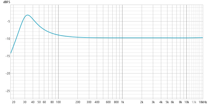
First, I measured the frequency response and self-noise, with the capsule replaced by a 39pF capacitor. You’ll find the noise plots further down below. The FR is flat in the midrange and high frequencies, but a clear peak of 7 dB is visible in the low frequencies. This could be due to poor component choices in the bootstrapping circuits for the diode biasing. MADON may have opted for inexpensive X7R MLCCs or other Class 2 ceramics, rather than the superior C0G capacitors. Class 2 ceramic capacitors exhibit a significant decrease in capacitance when bias voltage is applied across them. This decrease can be as high as 80%. There’s a significant voltage across C21 and C22, so their real capacity could be much lower than their nominal value when the microphone is powered. This capacitance reduction may also result in less attenuation of the noise from bias resistors R15 and R16, which could explain the high noise. I’ll talk about that later.
The MADON KM184 clone PCBA I had for testing was quite noisy, indeed. Below, you can see a comparison with the MXL991/MXL603 and one of my circuits, for which I chose the one with the lowest noise. This design also uses bias diodes, and if there were no circuit or component flaws, the KM184 should be more or less on par. The graph also includes the improvements that were achieved when some components were replaced. Note: the noise graphs show the output referred noise, though what counts is the input referred noise. The KM184 and my circuit have a gain close to 0 dB, so input and output referred noise are practically the same. The MXL has a gain of ~1.3dB, so the graph should be lowered by 1.3 dB to be comparable with the other graphs. However, there are such large differences between the noise levels that this is not relevant for the final conclusions. Each noise plot will be explained when discussing the modifications I made below.
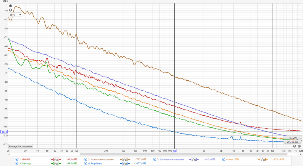
Noise density comparisons
OK, back to the mods that I carried out to reduce the noise. Given the concept of the impedance converter, designed as if it were a non-inverting Op-Amp with 0dB closed loop gain, it can be expected that components within the amplifier’s feedback loop will not contribute significantly to the total noise. After all, the strong feedback reduces any error generated within the feedback loop. Therefore, we should primarily focus on the components in the high-Z region before the impedance converter. These are:
1) Bias diodes D13 and D16, which could be leaky.
2) Bias resistors R15 and R16 inject noise into the circuit. But if C20 and C21 are chosen properly, they will short out the Johnson noise from these resistors to some low-impedance nodes in the circuit. Much in the same way as Johnson noise from GΩ bias resistors is shorted out to ground through the capsule capacitance. However, as I mentioned earlier, if said capacitors are undersized or of the wrong type, then the resistor noise will slip into the input circuit.
3) Poor-quality JFETs D14 and D15
As mentioned, correctly connecting C15 to ground didn’t improve the noise. That was a bit disappointing. All noise graphs shown further up were taken with C15 connected to ground. Let’s go through each noise graph one by one.
The top graph (brown) shows the first noise measurement that I took. Right after that, I also plotted the MXL603/MXL991 noise graph (red). A very obvious difference. Self-noise level of the KM184 clone measured -96.1 dBV (A), versus -112.5 dBV (A) for the MXL.
It took a while before I traced the schematic and started hunting for the noise source(s), but when I measured the KM184 clone again, the noise level was much lower compared to the first measurement (dark blue graph vs brown). It now measured -110.7 dBV (A), lagging only a few dB behind the MXL. I’m not sure why all of a sudden I measured so much lower noise levels, but they remained consistent after that, until I started modifying the circuit. What I did notice is that it takes up to two minutes for the noise to settle to its final level. Maybe I was measuring just after powering up the first time, I don’t know. In two minutes, I saw the noise going down by more than 10 dB, something I cannot remember having seen with other mic circuits. Anyway, this latest measurement of the unmodded PCBA is now my reference.
Next, I replaced bias diodes D13 and D16 with Nexperia BAV199 diodes. Unfortunately, no improvement. I haven’t included a graph, as it would look the same as the ref.
I then replaced capacitors C20, C21, and C22 with C0G types of the same value. This made a significant improvement! The noise floor has dropped to -118.4 dBV (A), so we’ve gained almost 8 dB! It is even a bit below the MXL noise floor. Now we’re getting somewhere!
The last modification I did was swapping out the JFETs. I bought BF862 JFETs from several different shops on Aliexpress. Some had the same font type and text on them as the ones on the MADON PCBA. I swapped out the JFETs for new ones with the same inscription, and guess what… an even further noise reduction down to -121.5 dBV (A)! The light-green graph shows the noise floor that I achieved with the mods described. It still lags my proprietary design by 2.5 dBV (A), but this is quite good. With this value and a noise-free capsule, you’d get a microphone with a 10 dB (A) self-noise level. I’m not sure about the KM184 capsule self noise level, but theoretically, a mic self noise level of 13 dB (A) could be realistic. This is an awesome result!
And what about the frequency response now that we have swapped out the input circuit capacitors for decent C0G types? Flat down to very low frequencies 😊.
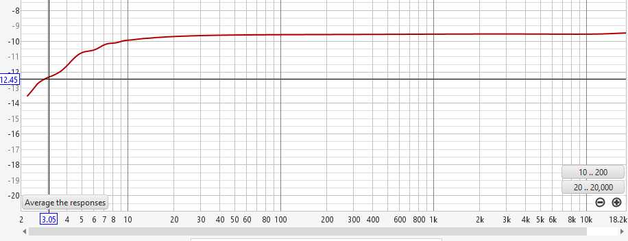
Frequency Response with CoG caps.
To conclude this section of mods & measurements, I wanted to share some Gain, THD, and headroom data that I measured on the modded PCBA:
Gain @ 100mV input voltage and with a 39 pF coupling capacitor: -0.53 dB
THD @ 100mV input voltage and with a 39 pF coupling capacitor: 0.0017% (-95 dB), 2nd harmonic only.
Maximum output level at 0.5% THD: 2.19 V. With a specified sensitivity of 15mV/Pa, this would yield a SPL limit of 137.3 dB. Neumann specifies 138 dB at an unknown THD level.
Conclusions
- The MADON KM184 PCBA is an almost exact copy of the Neumann KM184. And with the right quality components, its performance is probably on par with Neumann. In any case, the measured values were credible after modifications were carried out. The high self-noise was caused by the wrong type of capacitors in the input circuit and poor-quality JFETs.
- The circuit has a very low self-noise, though an even lower value should be feasible. Maybe with other components, but at least with other circuit topologies it is. It also has very low THD: more than an order of magnitude below e.g. Takstar CM-60 and CM-63 Schoeps style circuits, though it must be said that improvements in those circuits are possible with a properly biased JFET.
- The circuit concept with the stacked power supply on top of the impedance converter is quite uncommon, and I fail to see the benefits of this solution. Without stacking, the circuit becomes simpler, and the headroom can be increased.
What’s next…
Although the circuit is now pretty good, I’d like to explore and test whether the noise floor can be improved any further with other types of JFETs. And I’d like to try some of the other BF862 JFETs from other Aliexpress shops. Once I’ve done that, I’ll share the results here, including links to the Aliexpress shops.