Before I discuss the modifications of the UMC202HD, I would first like to say a few words about the choice of this Audio Interface. Because I did not want to spend a fortune on the Audio Analyzer, but was looking for a good price/quality ratio, after some research on the internet I came across the Behringer UMC202HD. I learned from this video by Julian Krause that the UMC202HD was among the best with respect to noise performance, which I considered one of the most important performance criteria. At least, it was much better than the more expensive Steinberg UM22 I already owned. And when I could get a used one for just €30 plus shipping, I decided this would be the Audio Interface to use for my project. Below you can see part of the table that Julian published, in which I added some prices of Audio Interfaces that were better than the UMC202HD.
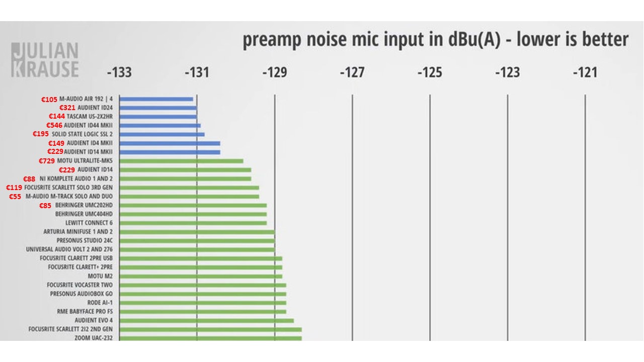
Once I decided on the UMC202HD and purchased it, I started figuring out how to bypass the input and output circuits. So I did a search on the Internet to see if others had already done the same and stumbled upon this thread on the diyAudio forum, where all kinds of modifications people have tried were discussed. You will find a number of posts from me as well (user jp8). Along the road, I noticed the UMC202HD contained some serious design flaws that I wanted to resolve. Once addressed, especially the THD and, to a lesser extent, the noise specs improved. You will find performance comparisons between the stock UMC202HD and the modified UMC202HD + my interface circuits here.
The circuit changes, as discussed in this forum, that eventually made it to my UMC202HD include:
- Bypassing the input and output circuits
- Killing the 48V boost converter
- Improving the internal LDO power supply
- Swapping the Op-Amps
- Modifications to the input and output circuits of the Codec chip (CS4272)
- Solving the oscillation of the Vcom buffer Op-Amp.
- Removal of the Clip and Signal LEDs, which were moved to the front panel of the Audio Analyzer from the UMC202HD front panel
There were other modifications proposed that perhaps could have improved the UMC202HD even further, but I did not test them as, at a certain moment, I was happy with the performance level improvements obtained with the modifications mentioned. Perhaps I will add a DAC output filter or improve the decoupling of the analog circuits, but that is not going to happen anytime soon.
In the diyAudio forum thread, you will also find a schematic of the analog section of the UMC202HD. See post #101 for the schematic shared. It has allowed other forum members, including me, to analyze the circuits, identify several design flaws, and come up with solutions for improvement. I have redrawn several parts of the analog section and included the modifications I’ve done in this circuit diagram. The complete schematic of the modified circuits can be downloaded here. The modified sub-circuits are also depicted individually in the sections below. While reading the text below, it may be convenient to have this schematic and the one from post #101 at hand. And finally, the CS4274 datasheet and Application Note AN241 from Cirrus Logic about analog Input Buffer circuits for ADCs.
The following paragraphs cover all the modifications in more detail. If you want to do all the mods, you will need the following parts, which are readily available from, e.g. Mouser or Digikey:
2 x OPA1664AID or OPA1664AIDR
The resistors listed below are either Thick Film or Thin Film (Thin Film is more stable, has lower excess noise, but is more expensive and more sensitive to cracking.)
1 x Resistor 30k9 0603 1% (Alternatively 84k5. Read the “Internal power supply modification” section below.)
4 x Resistor 91R 0603 1%
3 x Resistor 100R 0603 1%
8 x Resistor 4k7 0603 1%
2 x MLCC 390pF 0603 5% 50V C0G/NP0
2 x MLCC 2N7 0805 5% 50V C0G/NP0
4 x 47R 1% Metal Film, through-hole resistors
4 x BAT41 Schottky Diodes
Lower-tolerance parts can be used, of course. The working voltage of the MLCCs can be chosen lower, but 50V is probably more commonly available.
1 x Solder lug with ~3.5mm hole to connect the output XLR cable shield to Ground.
Some thin microphone cable, e.g. Tasker C280, for input and output wiring.
AWG24 or AWG26 hookup wire for the LED wiring.
In the paragraphs below, I have included pictures of the UMC202HD PCBAs to mark the modifications. These pictures were taken from a second unmodified UMC202HD I have. I’m sorry, but I don’t feel like opening up my ready-made analyzer to take pictures right now of the actual modifications. I hope you’ll understand.
Bypassing the input and output circuitry:
When using an Audio Analyzer, you don’t want to be limited to the ~1V input and output voltage range of a stock UMC202HD, or any other Audio Interface for that matter. So you want to add external, calibrated fixed-gain amplifiers and attenuators to the inputs to obtain a wider measurement range of maybe up to 200V. Because gain or attenuation are fixed and calibrated, it is no longer necessary to calibrate the setup for each voltage measurement. Secondly, you’ll also want adjustable line and power amplifiers as outputs. Once these circuits have been added externally to the Audio Interface, you basically no longer need the preamp and output circuits of the Audio Interface. So we can bypass the preamp and line input/output circuits of the UMC202HD and also improve noise and distortion performance. The signals from and to these new external input and output circuits will be routed directly to the input filter and output buffer of the Codec chip as depicted in the block diagram above. Let’s first look at how to bypass the input circuitry.
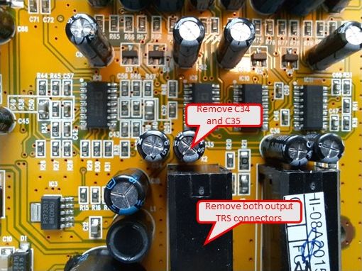
As you can see on the schematic of the ADC buffer, the signals to the ADC input buffer circuits are AC-coupled through C34 and C35. These capacitors can be removed if the outputs of the external input circuits are AC-coupled (which they are). The + side of C34 and C35 attaches to the ADC buffer Op-Amps, so we can use the + solder pads to connect a microphone cable to the external input circuit. If you remove the TRS output connectors, you can feed the microphone cables through the holes in the back of the UMC202HD housing. And you can solder the shields of the microphone cables to the TRS ground pin. The picture below shows where to find C34 and C35 next to the TRS connectors. The callout points to C35, with C34 being to the left of this capacitor.
Important update: The output level of the Line-Output can exceed the maximum input voltage of IC8B and IC8D. I’ve had this several times now when the input was overloaded, resulting in a temporarily “dead” ADC input channel. There should be clamping diodes on these inputs, not shown in the schematic further down in this chapter. At the time of writing, I have yet to add them, so I could not prove they would actually solve the issue or not. The schematic is below. Simulations revealed that with the components selected the expected input current into the + inputs of IC8 will be lower than 1 mA. The maximum allowed is 10 mA. So this should work.
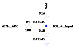
Now let’s move on to the output buffer connection, which connects to the adjustable external output buffers. First, we need to unscrew the riser board and remove the output level potmeter VR1. While not strictly necessary, I would recommend removing switch SW1 as well. If you accidentally leave it engaged, the signal will be slightly attenuated. Now that the potmeter has been removed and looking from the BACKSIDE of the potmeter, you can short out the center and the right pin of each of the potmeter sections. If you do not short out the center and the right pins, then IC11 Op-Amp inputs 3 and 5 are left floating and would cause oscillations of these Op-Amps. See the blue dots depicted on the potmeter housing in the picture below. The microphone cable to the external output circuits connects to the left pads of the potmeter.
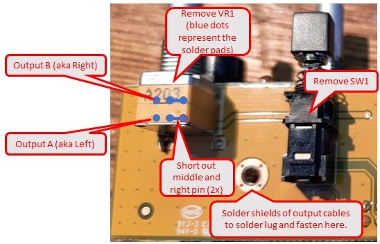
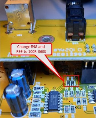
Removal of VR1 and SW1. Connect output cables here. Underneath the riser board, swap R98 and R99 with 100R 0603 resistors.
Last, but not least, we need to swap two resistors on the main board. These are 1k resistors R98 and R99, which have to be changed to 100R to prevent too much attenuation by the 10k external potmeter of the external output circuit. You will find these resistors underneath the riser board, so they have to be swapped before reassembling the riser board. (Note: see also the removal of Signal and Clip LEDs in the last paragraph, which you may want to do while the riser board is still off the main board.)
Killing the 48V phantom power supply circuit:
Many people report a spike in the 15kHz-25kHz range. Mine had a 17 kHz spike with a level of around -90 dBfs or so. Unfortunately, I forgot to take a screenshot of the FFT showing this anomaly. But I found this picture on the web where this spike is clearly visible, just above 20 kHz (white trace = UMC202HD). As this signal was also present when no signal was applied to the inputs, it had to originate from the UMC202HD hardware. I suspected the 48V phantom power boost converter (IC2) and this proved to be right. When I disabled it, the spike was gone. Because I had already planned to build an external 48V phantom supply, I decided to remove the boost converter IC and I shorted the Gate and Source of the switching MOSFET (T2). Problem solved. Other people just removed L5, having the same effect. With only L5 removed, I wasn’t sure whether the boost converter would still be switching and would still cause a spike. So I decided to remove IC2 instead and keep the MOSFET off by shorting out the Gate and Source. The picture below shows the modifications, including a decoupling capacitor upgrade (C16). The original elcap was replaced by a low-ESR OSCON capacitor to improve noise and ripple reduction of the 5V USB power. I don’t know if it made any sense, but I had it lying around and decided to use it here.
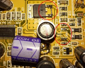
Disabling the 48V phantom power supply: removal of IC2 and Gate and Source of T2.
Internal power supply modification:
A second issue I noticed with the UMC202HD was the fact that THD was rising sharply at input levels above -6 dBFs. Not exactly what you would like to see in an Audio Analyzer, where you want maximum dynamic range. Although one can expect rising HD levels close to 0 dBFs, I tried to find ways to reduce the distortion. The first suspects were the Op-Amps, but the AD8694 Op-Amps utilized in the UMC202HD are rail-to-rail output types and the input voltage range was also not exceeded, albeit only just so. But what did worry me was the fact that the internal power supply voltage was only 4.5V, even when the Audio Interface was powered with exactly 5V USB voltage. Even on the CS4272 AD/DA chip, which according to the datasheet requires a 4.75 to 5.25V power supply range, there was just 4.5V. So somewhere in the circuit, 0.5V got lost. A flagrant design flaw, in my opinion.
I figured out there was an LDO circuit (IC3, TPS72301) powering the analog circuits. Its output voltage was set to 4.5V by means of resistors R16 and R17. I changed the resistor values and set the output voltage to 4.9V, which reduced THD dramatically at levels above -6dBFs! Unfortunately, I lost my before/after comparison measurement data, but at the end of this section, you will find RTA plots at different levels of an original UMC202HD and of the modified UMC202HD, including the Audio Analyzer input and output circuits in the loop. The improvements are quite obvious, I would say.
Of course, the 4.9V mod will only work if your USB voltage on the UMC202HD board measures 4.95V or higher! If yours is lower, you may want to check your USB cables for high losses. Anyway, as I will power the UMC202HD through a separate power supply connected to the USB Isolator, I have full control over the actual USB voltage. I actually adjusted the power supply to 5.15V. This is still within USB requirements and gives the audio circuits a bit more headroom.
If you want to change the LDO output voltage to 4.9V as I did, you can change the value of R17 to 30k9. This is the easiest way. Alternatively, you may want to move R17 to the position of R16 and change R16 to 84k5. According to the datasheet, R16//R17 should be equal to 19k, ideally. It will make the circuit a few mV more accurate, but that hardly makes sense in this case. In the picture below, you can see where R17 is located. The schematic shows the complete LDO circuit for your reference. You may also want to swap C16 and C18 and use better low-ESL, low-ESR or OSCON types.
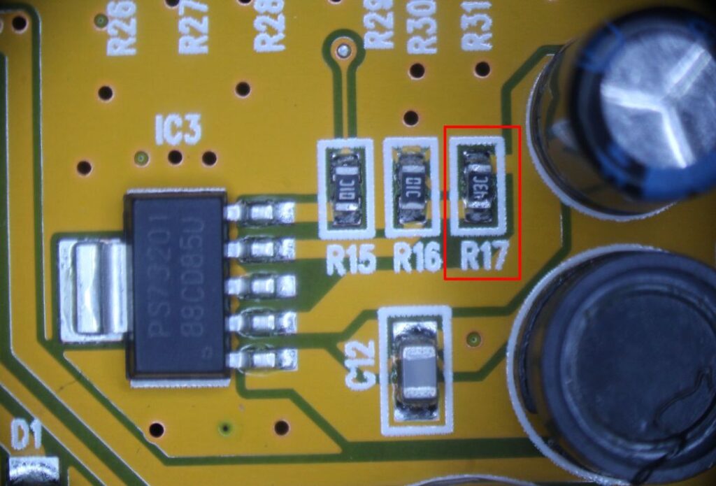

Setting the LDO output voltage to a higher voltage, e.g. 4.9V, by changing R16 and/or R17 values.
Swapping the Op-Amps:
In a budget Audio Interface, you cannot expect it to have top-of-the-bill Op-Amps. Although the Analog Devices AD8694 is a very good Op-Amp, there is a somewhat better candidate, which is TI/Burr-Brown’s OPA1664. It has slightly lower noise, a bit better dynamic range, and an order of magnitude lower distortion, which are all plusses in an Audio Analyzer, especially in this circuit operating from less than 5V. I decided to use this Op-Amp to replace IC8 and IC13, which are the AD/DA converter input and output filter/buffer stages. Unfortunately, I do not have before/after noise and distortion measurement plots to show the effects of this mod.
You can use Chip Quik SMD1 and a heat gun set to 250 °C (480 °F) to effortlessly remove the ICs, without overheating or damaging other parts. Thanks to the relatively low airflow temperature, you will not accidentally blow off small SMTs adjacent to the ICs involved. It’s not cheap, but you will need only very little of this solder, which might save you a lot of aggravation. If you do not want to use Chip Quick, you’ll probably need to set the airflow temperature to somewhere in the 380-400 °C (~715-750°F) range. The picture below shows the location of the two Op-Amps involved.
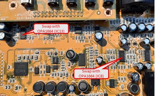
Swapping the AD8694 Op-Amps with slightly better OPA1664 Op-Amps.
Modifying the input and output circuits of the Codec chip (CS4272):
These are probably the most drastic modifications on the board as you will have to cut a number of tracks with the risk of damaging surrounding parts or tracks. But the changes are worth the effort. Let’s take a closer look at the ADC Input Buffer circuit first. Below, you will see two pictures: the first one shows the single-ended ADC Input Buffer from the Cirrus Logic AN241 Application Note and the other one shows the UMC202HD ADC Input Buffer circuit.
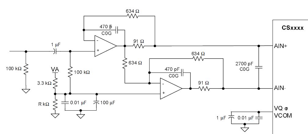
ADC Input Buffer circuit, recommended by Cirrus Logic AN241 Application Note.
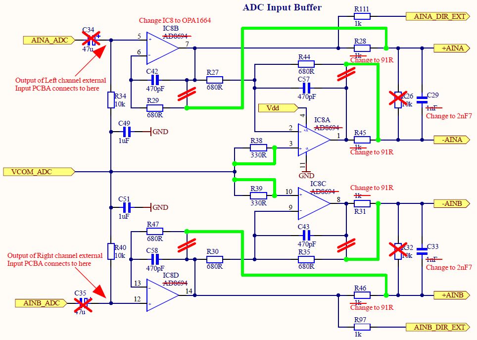
The Behringer ADC Input Buffer circuit, including all the modifications.
Clearly, there are similarities, but also differences. As the internal signal path of the UMC202HD is unbalanced, Behringer chose the Single Ended circuit from the AN241 Application Note, rather than the differential datasheet circuit. But they haven’t implemented the circuit properly, in my opinion, and seemed to totally miss the point of the AN241 circuit. When you read chapters 3.3 and 3.4, you will understand what I mean. Whether this was an intentional modification, perhaps to prevent oscillations, I don’t know. Anyway, I decided to swap the Op-Amp with an OPA1664 and restore the AN241 circuit. This worked well, although I must admit I did not check the circuit for overshoot and stability. It worked, and I was satisfied.
I later started to contemplate the circuit again. In the diyAudio thread, it was suggested that using an AD8694 in the AN241 circuit could cause oscillations, as CMOS outputs tend to have a rather high open-loop output impedance. The In-The-Loop compensation technique applied in the AN241 circuit requires the output impedance Zo to be significantly smaller than R29 (or R47). With the Zo of the AD8694 being in the order of 100 Ohm, I would not call this “significantly smaller”, so this could indeed be a real issue. The Zo of the OPA1664 is roughly 50% of the AD8694 Zo, so it could indeed be more stable. I didn’t breadboard the AN241 circuit with the AD8694 and the OPA1664, but I did run some simulations with spice models supplied by the manufacturers, which also model Zo. However, the simulations did not reveal a lot of difference in overshoot between the two Op-Amps (~20-25%). I played around with some different component values to examine the effects on stability, but not a lot changed, actually. Overshoot could be further reduced by increasing the capacitance of C42 and C58 to e.g. 1nF. So I decided to leave the circuit as it is (i.e. AN241 circuit with OPA1664) and not try to improve it any further.
The two pictures below show how to make the changes from the schematic on the PCBA. The top one shows the components to replace or swap. The second picture shows the trace cuts and patch wires around IC8.
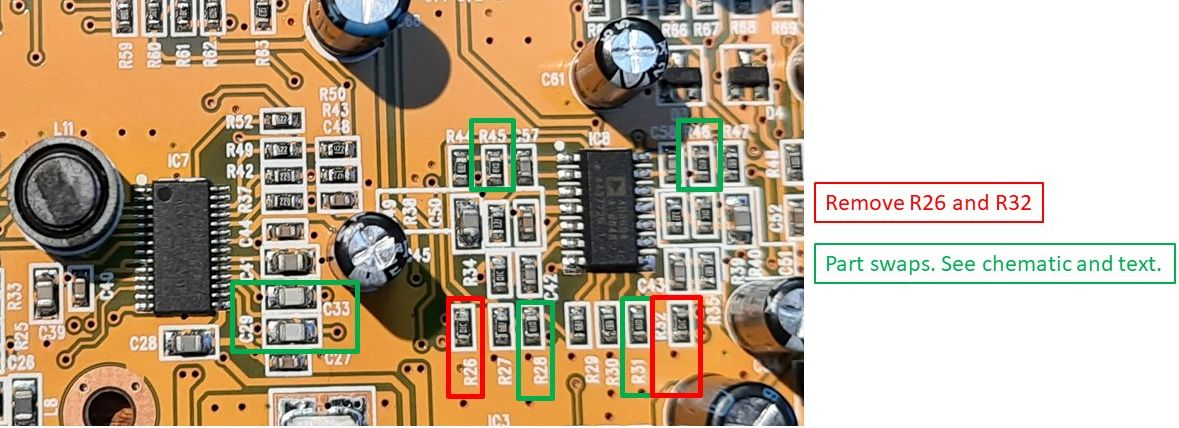
Parts to remove or swap.
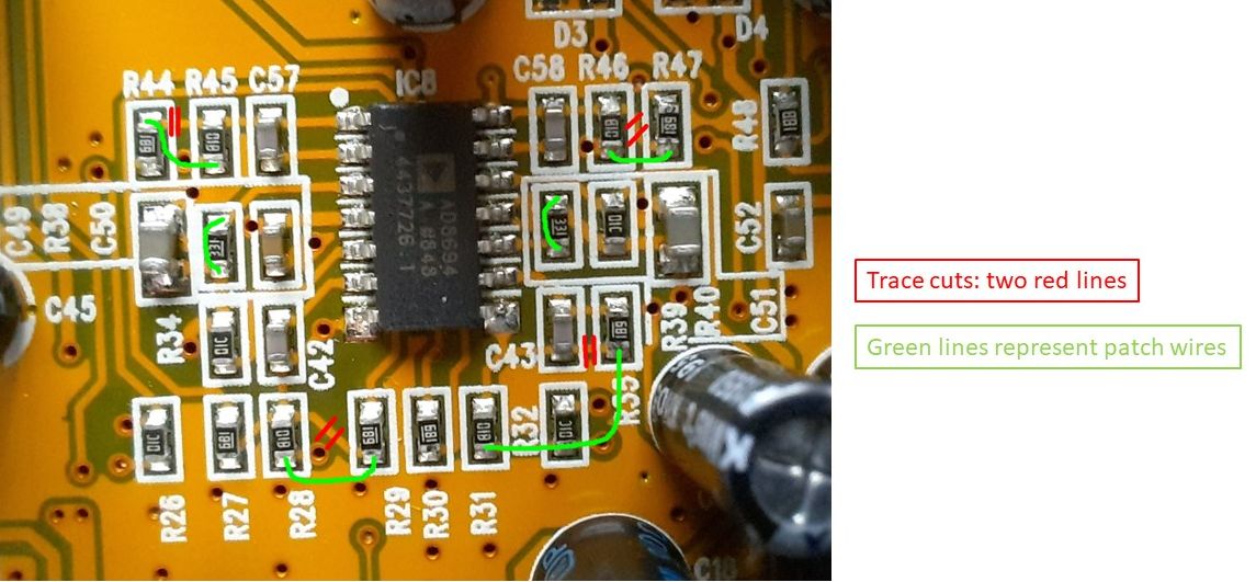
ADC Input Buffer modifications: trace cuts and patch wire connections.
Now let’s move on to the Output Buffer circuit around IC7. Again, two circuits will be shown: one with the circuit Cirrus Logic had in mind and which comes from the CS4274 datasheet, and the other with the Behringer schematic, including the modifications.
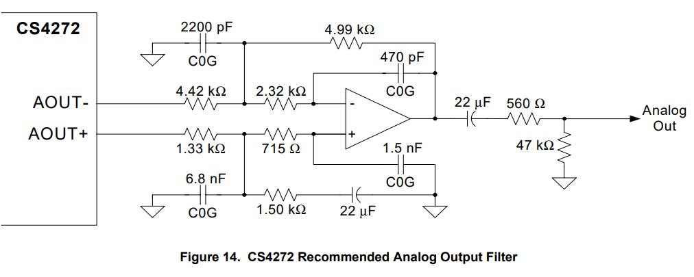
The CS4272 Recommended Output Filter/Buffer circuit from the datasheet.
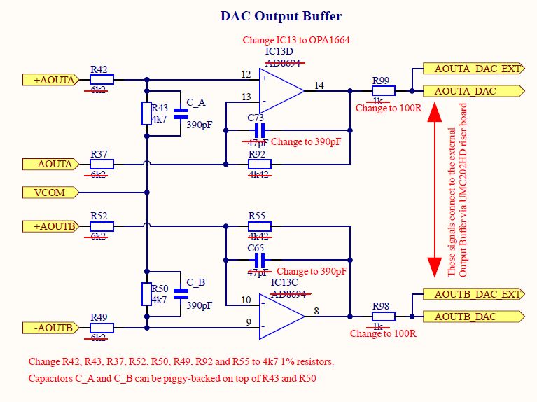
The UMC202HD output filter/buffer circuit, including all modifications.
Unfortunately, Behringer decided to leave out any (significant) low-pass filtering from the output buffer stage. Probably to save some money, assuming nobody will hear the out-of-band noise caused by the DAC Noise-Shaping. Admittedly, good audio circuits should be able to handle > 20 kHz signals without distortion, but good design practice is to always limit the bandwidth of your circuit to just a little more than your in-band signal bandwidth. So I decided to try and improve the circuit as best as possible without making too many invasive modifications. So I decided to increase the values of C73 and C65 significantly and add C_A and C_B, which changed the circuit into a 6dB/oct 87 kHz LPF filter. This modification reduces the RMS noise level by approximately 50%. It’s a significant improvement, and although visually on the oscilloscope it doesn’t do much, for the time being, it’s good enough for me. Maybe I will add another filter later. Just as test, I made a simple 2nd-order LC filter with a small ripple, which compensates for the slight signal loss at 20 kHz due to the 6 dB/oct filter. The result can be seen below. I decided to not include this filter between the UMC202HD output and the analyzer output driver because it introduced a tiny amount of extra 3d harmonic distortion due to the ferrite cores of the inductors. I did not want to change something that I considered a non-issue with a new one, when most of the time I will watch the input signals in an FFT up to 20 kHz and this noise is out-of-band.
The pictures below show the noise levels on the output of a stock UMC202HD (left) and on the output of the audio analyzer (right) using the modified UMC202HD. Noise is reduced to ~6.8mV RMS, from ~12.9mV RMS of the stock soundcard.
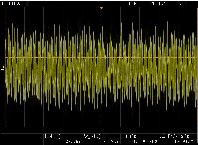
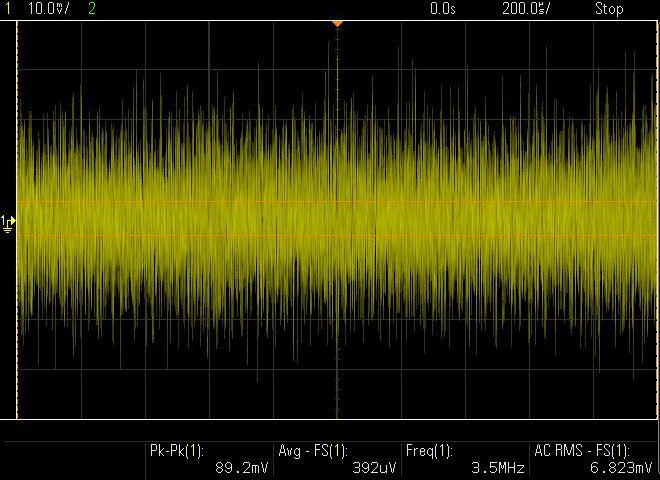
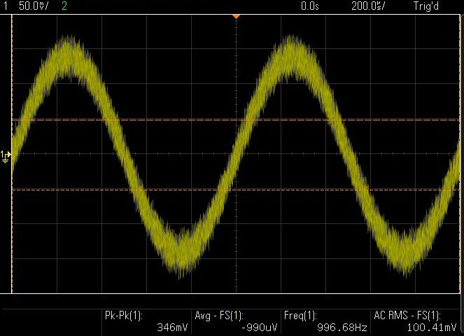
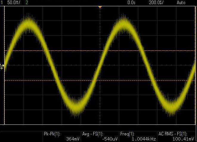
Output noise levels of a stock UMC202HD (left) and the modified circuit (right). Visually, not a lot different, but the AC RMS values in the bottom right corner of the noise pics speak for themselves.
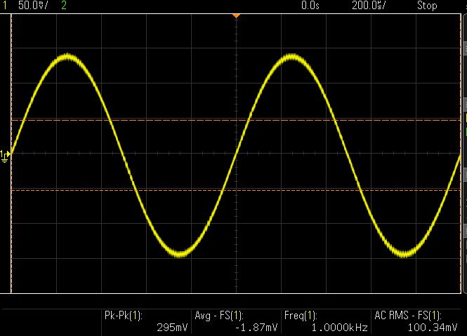

And this is what a sine wave looks like when run through an extra 12 dB/oct filter as pictured on the right.
Again, we conclude this section by showing a picture of the modifications on the PCBA.
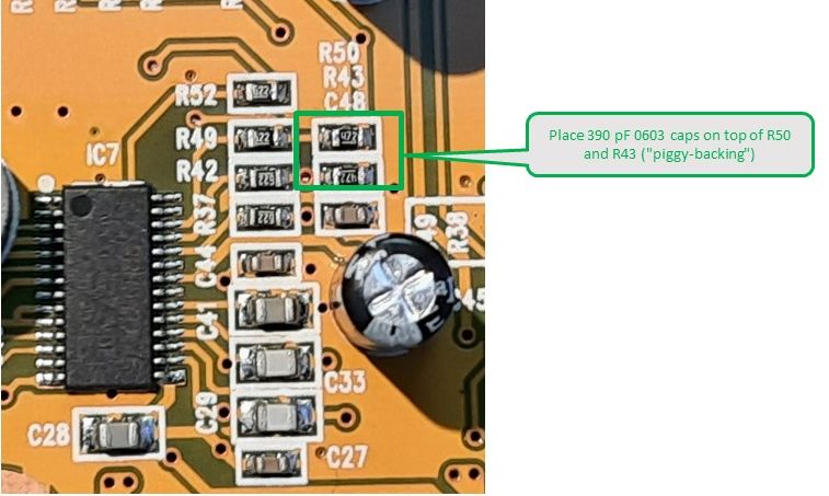
DAC Output Buffer/Filter Modifications on the PCBA.
Solving the oscillation of the Vcom buffer Op-Amp:
In the diyAudio thread mentioned earlier, in post #553 , the author mentioned he found that the Vcom buffer IC16B was oscillating at 140kHz, which was due to the capacitive load of C49 and C51. Although I did not notice any anomalies in the REW measurements that could be related to this oscillation, the oscillation is objectionable and just should not be there. I solved the oscillation of the Vcom buffer Op-Amp by inserting a 100R resistor between the IC16B output and the capacitors. This required lifting pins 6 and 7 of the IC, which should be done carefully as they break off quite easily. I soldered a 0603 resistor between these shorted pins and the solder pads on the PCB. The picture below shows where to find these pins.
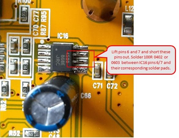
Lifting of pins 6 and 7 to insert a 100R resistor.
Removal of the Signal and Clip LEDs:
Although one can do without the Signal and Peak LEDs when using the UMC202HD in this application, they can be convenient to have. While measuring, you can easily see in the corner of your eye if there is a (significantly high) signal or when the ADC clips. So I removed the LEDs from the PCBA and mounted some 5mm LEDs between the XLR inputs and Range selector switch. The picture below shows how the Cathodes and Anodes of the LEDs are wired to the PCBA.
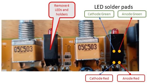
Location of the LEDs and their Cathodes and Anodes.
Other modifications:
As I already mentioned in the introduction of this chapter, a lot of modifications were discussed in this thread on the diyAudio forum, from which I made a selection based on what I expected to be relevant in the context of this application. But there are several other potentially interesting mods being suggested there, a.o. an output filter (though I would prefer to just replace the so-so output buffer circuitry on the UMC202HD board with the datasheet circuit), per-chip power supply decoupling with ferrite beads, and even an auto-ranger circuit. I would say: take a beer, sit back and spend a night reading all the 30+ pages of the thread, and take out the good bits.
This concludes the UMC202HD modifications chapter. If you ever plan on modifying a UMC202HD, I hope this information is helpful to you. Now let’s move on to the front-end and back-end circuits of the analyzer in the next chapters…